Example Platform Microwave Oven Control
Worst Case Analysis
|
REVISION CORRELATION CHART |
|||||
|
REV LTR |
ECN NO. |
REVISION |
REV’D BY |
APPV’D |
|
|
|
|
|
|
|
|
|
|
|
|
|
|
|
|
|
|
|
|
|
|
|
|
|
|
|
|
|
|
|
|
|
|
|
|
|
|
|
|
|
|
|
|
|
|
|
|
|
|
|
|
|
|
|
|
|
|
|
|
|
|
|
|
|
|
|
|
|
|
|
|
|
|
|
|
|
|
|
|
|
|
|
|
|
|
|
|
|
|
|
|
|
|
|
|
|
|
Table of Contents
1 PURPOSE......................................................................................................... 6
2 Block Diagram........................................................................................... 7
2. 1 AC Input.................................................................................................... 7
2. 2 DC Power Supply...................................................................................... 7
2. 3 AC on DC.................................................................................................. 8
2. 4 CPU, EEPROM......................................................................................... 8
2. 5 Oscillator.................................................................................................. 8
2. 6 Safety Circuit............................................................................................ 8
2. 7 KEYPAD.................................................................................................... 8
2. 8 Display, LED’s.......................................................................................... 8
2. 9 Piezo Speaker............................................................................................ 8
2. 10 Door Switch.............................................................................................. 9
2. 11 Combi Return Switch................................................................................ 9
2. 12 Fans, Lights.............................................................................................. 9
2. 13 Mag 1 Triac.............................................................................................. 9
2. 14 Mag 2, Front Triac................................................................................... 9
2. 15 Mag 3, Rear Triac..................................................................................... 9
2. 16 Relay Enable............................................................................................. 9
2. 17 60Hz Reference......................................................................................... 9
2. 18 Voltage Sense, Factory Options............................................................... 9
2. 19 208/240 DLB relays, 19a, 19b, 19c, 19d................................................ 10
2. 20 TCO......................................................................................................... 10
2. 21 Current sense.......................................................................................... 10
2. 22 RTD PWM............................................................................................... 10
3 Extreme Control Conditions............................................................ 11
3. 1 Line Voltage Extremes............................................................................ 11
3. 2 Operating Temperature.......................................................................... 11
4 Control Worst Case Analysis............................................................. 11
4. 1 AC Input...................................................................................................... 11
4.1.1 Worst Case Scenarios............................................................................. 11
4.1.1.1 208V/240V, 60Hz transformer................................................................ 12
4.1.1.1.1 T1, 180V, 60Hz. What is –Vunreg,..................................................... 12
4.1.1.1.2 T1, 264V, 60Hz. What is winding temperatures................................. 13
4.1.1.1.3 T1, 264V, 60Hz. What max -Vunreg................................................... 13
4.1.1.2 230V, 50Hz transformer......................................................................... 13
4.1.1.2.1 T1; 230V, 50Hz, max temperature...................................................... 13
4.1.1.2.2 T1; 230V, 50Hz, power sufficiency..................................................... 14
4. 2 DC Power Supply........................................................................................ 14
4.2.1 Worst Case for D1-D4............................................................................ 15
4.2.2 Worst Case for C4.................................................................................. 15
4.2.3 Worst Case for Q1.................................................................................. 15
4.2.4 Worst Case for R53................................................................................. 17
4.2.5 Worst Case for Q6.................................................................................. 17
4.2.6 Worst Case for R54................................................................................. 17
4.2.7 Worst Case for R55................................................................................. 17
4.2.8 Worst Case for L1................................................................................... 18
4.2.9 Worst Case for D25............................................................................ 19
4.2.10 Worst Case for D26............................................................................ 19
4.2.11 Worst Case for C6.............................................................................. 20
4.2.12 Worst Case for Z4............................................................................... 20
4.2.13 Worst Case for R56............................................................................. 21
4.2.14 Worst Case for Z1............................................................................... 21
4.2.15 Worst Case for D27............................................................................ 21
4.2.16 Worst Case for C1.............................................................................. 22
4.2.17 Worst Case for Q11............................................................................ 23
4.2.18 Worst Case for D24............................................................................ 23
Voltages VR, Vdisp:................................................................................... 23
4.2.19 Worst Case for Z2............................................................................... 23
4.2.20 Worst Case for R4............................................................................... 24
4.2.21 Worst Case for R3............................................................................... 25
4.2.22 Worst Case for Q2.............................................................................. 25
Voltages VCC:............................................................................................ 25
4.2.23 Worst Case for C2.............................................................................. 25
4. 3 AC on DC.................................................................................................... 26
4.3.1 Worst Case for R15................................................................................. 26
4.3.2 Worst Case for Q3.................................................................................. 26
4. 4 CPU............................................................................................................. 27
4.4.1 Worst Case for R78, R79........................................................................ 27
4.4.2 Worst Case for R103............................................................................... 28
4.4.3 Worst Case for C12................................................................................ 28
4.4.4 Worst Case for U1.................................................................................. 29
4.4.5 Worst Case for U7.................................................................................. 32
4.4.6 Worst Case for R66................................................................................. 32
4. 5 Oscillator.................................................................................................... 33
4.5.1 Worst Case for Y1................................................................................... 33
4.5.2 Worst Case for R91................................................................................. 34
4. 6 Safety Circuit.............................................................................................. 34
4.6.1 Worst Case for block functionality........................................................ 34
4.6.2 Worst Case for R61................................................................................. 35
4.6.3 Worst Case for R81................................................................................. 35
4.6.4 Worst Case for C14................................................................................ 36
4.6.5 Worst Case for C16................................................................................ 36
4.6.6 Worst Case for R22................................................................................. 37
4.6.7 Worst Case for D17................................................................................ 37
4.6.8 Worst Case for C17................................................................................ 37
4.6.9 Worst Case for R80................................................................................. 38
4.6.10 Worst Case for D18................................................................................ 38
4.6.11 Worst Case for D19................................................................................ 38
4. 7 Keypad........................................................................................................ 39
4.7.1 Worst Case for R23 – R29..........................................................................
4.7.2 Worst Case for R6 – R12........................................................................ 39
4.7.3 Worst Case for D5 – D7......................................................................... 40
4.7.4 Worst Case for Keypad resistance......................................................... 40
4.7.4.1 Keypad resistance................................................................................... 40
4. 8 Display/LED............................................................................................... 40
4.8.1 Worst Case for DS1................................................................................ 40
4.8.2 Worst Case for R13, R14........................................................................ 41
4.8.3 Worst Case for RN1, RN2....................................................................... 41
4.8.4 Worst Case for R100, R104.................................................................... 42
4.8.5 Worst Case for R101............................................................................... 42
4.8.6 Worst Case for R102, R103.................................................................... 42
4.8.7 Worst Case for Q12................................................................................ 42
4.8.8 Worst Case for Q13................................................................................ 43
4. 9 Piezo Speaker.............................................................................................. 44
4.9.1 Worst Case for R21, R49............................................................................
4.9.2 Worst Case for R18, R19........................................................................ 44
4.9.3 Worst Case for R16................................................................................. 44
4.9.4 Worst Case for R17................................................................................. 45
4.9.5 Worst Case for Q4.................................................................................. 46
4.9.6 Worst Case for Q5.................................................................................. 46
4.9.7 Worst Case for Y101............................................................................... 46
4.9.8 Worst Case for R101, R104.................................................................... 46
4.9.9 Worst Case for R102............................................................................... 47
4.9.10 Worst Case for R103............................................................................... 47
4.9.11 Worst Case for Q101.............................................................................. 47
4.9.12 Worst Case for D101.............................................................................. 48
4. 10 Door Switch................................................................................................ 48
4.10.1 Worst Case for R1............................................................................... 48
4.10.2 Worst Case for R50............................................................................. 48
4.10.3 Worst Case for D13............................................................................ 49
4. 11 Combi Return.......................................................................................... 49
4.11.1 Worst Case for D15............................................................................ 49
4.11.2 Worst Case for R2............................................................................... 49
4.11.3 Worst Case for R69............................................................................. 50
4. 12 Fans, light............................................................................................... 50
4.12.1 Worst Case for R97 – R99.................................................................. 50
4.12.2 Worst Case for K1 – K3...................................................................... 52
4.12.3 Worst Case for U3.............................................................................. 52
4.12.4 Worst Case for Z3............................................................................... 52
4. 13 Mag 1 Triac............................................................................................ 53
4.13.1 Worst Case for U3.............................................................................. 53
4.13.2 Worst Case for R94............................................................................. 53
4.13.3 Worst Case for R59............................................................................. 54
4.13.4 Worst Case for U4.............................................................................. 54
4. 14 Mag 2/Front Triac.................................................................................. 55
4.14.1 Worst Case for U3.............................................................................. 55
4.14.2 Worst Case for R95............................................................................. 55
4.14.3 Worst Case for R60............................................................................. 55
4.14.4 Worst Case for U5.............................................................................. 55
4. 15 Mag 3/Rear Triac................................................................................... 55
4.15.1 Worst Case for U3.............................................................................. 55
4.15.2 Worst Case for R96............................................................................. 55
4.15.3 Worst Case for R65............................................................................. 55
4.15.4 Worst Case for U6.............................................................................. 55
4. 16 Relay Enable........................................................................................... 56
4.16.1 Worst Case for R72............................................................................. 56
4.16.2 Worst Case for R73............................................................................. 56
4.16.3 Worst Case for R83............................................................................. 57
4.16.4 Worst Case for R84............................................................................. 57
4.16.5 Worst Case for R92............................................................................. 58
4.16.6 Worst Case for R93............................................................................. 58
4.16.7 Worst Case for C11............................................................................ 58
4.16.8 Worst Case for C18............................................................................ 58
4.16.9 Worst Case for D20............................................................................ 59
4.16.10 Worst Case for D21............................................................................ 60
4.16.11 Worst Case for Q9.............................................................................. 60
4.16.12 Worst Case for Q10............................................................................ 61
4.16.13 Worst Case for D16............................................................................ 61
4.16.14 Worst Case for R70............................................................................. 62
4.16.15 Worst Case for R71............................................................................. 62
4. 17 60Hz Reference....................................................................................... 62
4.17.1 Worst Case for R82............................................................................. 63
4.17.2 Worst Case for C15............................................................................ 63
4. 18 Voltage sense.......................................................................................... 63
4.18.1 Worst Case for R62............................................................................. 63
4.18.2 Worst Case for R63............................................................................. 64
4.18.3 Worst Case for R64............................................................................. 64
4.18.4 Worst Case for C19............................................................................ 64
4. 19 208V/230V Mag/ Kal rod relays drive................................................... 65
4.19.1 Worst Case for R51, R52, R66............................................................ 65
4.19.2 Worst Case for R57, R58, R106.......................................................... 66
4.19.3 Worst Case for Q7, Q8, Q14............................................................... 66
4.19.4 Worst Case for D10 – D12, D14......................................................... 66
4.19.5 Worst Case for D22, D23................................................................... 67
4.19.6 Worst Case for K4 – K9...................................................................... 67
4. 20 TCO......................................................................................................... 68
4.20.1 Worst Case for R75............................................................................. 68
4.20.2 Worst Case for R76............................................................................. 68
4.20.3 Worst Case for TCO switch................................................................ 69
4. 21 Current Sense.......................................................................................... 69
4.21.1 Worst Case for U20............................................................................ 69
4.21.2 Worst Case for R20............................................................................. 69
4. 22 RTD PWM............................................................................................... 71
4.22.1 Worst Case for R77............................................................................. 71
4.22.2 Worst Case for R74............................................................................. 71
4.22.3 Worst Case for RTD............................................................................ 71
4.22.4 Worst Case for C10............................................................................ 71
4.22.5 Worst Case for R67............................................................................. 72
4.22.6 Worst Case for R68............................................................................. 72
5 Appendices................................................................................................. 72
6 Notes Regarding worst case analysis........................................................ 72
To ensure that every component will withstand the most electrically, mechanically, and environmentally stressful situation that each component can be expected to endure – a worst case analysis. This Worst Case Analysis for the yyyyy Platform microwave oven is derived using the 043-00466 schematic and Bill of Materials according to 100-01153-00.
Below is a block diagram of the Platform control. Following this is a brief description of each block.
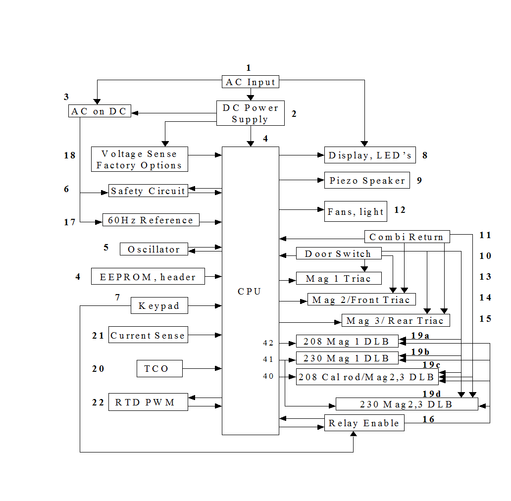 |
Block Descriptions
The AC Input is a step-down, isolation power transformer that provides a 29V – 59V ac source for the rectifier for the DC supplies and also a 3.2Vac-4.69Vac for the filament voltage for the VF display as the line voltage goes from the lowest value of 180Vac to 264Vac, respectively.
The DC Power Supply provide four voltages for the unit:
-Vunreg -29Vdc to - 58Vdc unregulated, filtered supply. This is sensed by the Voltage Sense block, block 18, to inform the micro which line voltage the control is plugged into, 208Vac or 240Vac
-VR -24Vdc regulated supply, power supply to the relays, triacs, display, speaker, and keyboard.
-Vdisp -29Vdc regulated supply, power supply for the safety circuit, and display grid cut off voltage.
-VCC -5Vdc regulated supply, power supply for the micro and the EEPROM.
The AC on DC block provides a temporary short to –VR once every line cycle. It provides a signal to the micro to indicate the frequency of the line so that the micro can fire the relays at the right time of the phase to increase relay life. It also will reset the micro if the micro is not active.
The CPU contains the microprocessor and the EEPROM. It accepts the inputs and processes the logic and provide the correct outputs.
The oscillator is a quartz crystal and a 1MW resistor designed to oscillate at 8MHz.
The Safety circuit alternates between ground and –VCC to pump up the voltage of a capacitor which when discharged, allows the microprocessor to reset if the micro should stop toggling the Safety circuit because it has stopped executing expected program instructions.
The Keypad provides START, RESET, Program, and Numeric entry into the control to cause various cooking times and modes.
The display is a Vacuum, Florescent Display with 9
grids of at most 9 anodes to indicate the various operational modes. The VF
display also requires a filament voltage that is supplied from the AC Input
transformer. The LED’s that indicate the mode of operation are multiplexed with
the display grids. The micro does not fire any display grids when the LED’s are
pulsed. Instead, Q12 or Q13 are fired in order to pulse an LED.
The Enunciator is a piezo electric device driven directly from the micro or thru resistors and can be supplied from the micro with 3 levels of power output, low, medium, and hi.
The Door Switch provides double protection against magnetron operation if the door of the microwave oven is open. The Door Switch normally shorts to circuit ground to complete the circuit path for the relays and the Optos. If the door is open, the Door Switch will interrupt current directly to the magnetron through the wiring harness. And an open door switch will also interrupt the drive circuits to the relays that operate the magnetrons. All this prevents the magnetrons from operating with the door open.
The Combi Return is permanently hardwired to ground only in the Combi oven. Otherwise, in the 3TC oven, the Combi Return permanently floats open.
The relays for the cooling fan and the light are activated through the inverting buffer, U3. There is no safety concerns if these devices operate continually or operate when the door is open. Either CF208 or CF230 are activated, but never both at the same time. Which one can be turned on is determined at start up when the micro measures what line voltage is present.
In a valid cooking mode, the micro turns ON the Opto, U4, whether in a 3TC model or a Combi model. The Door must be shut in either case before the Opto will activate. The Optoisolated triacs provides power to the microwave oven’s magnetron for those units that can operate the magnetron with a programmable duty cycle to provide various power levels of cooking.
This output activates Magnetron 2 when the control is installed in a 3TC oven; it activates the Front Cal rod when the control is installed in a Combi oven.
This output activates Magnetron 3 when the control is installed in a 3TC oven; it activates the Rear Cal rod when the control is installed in a Combi oven.
The Watch Dog circuit acts to shut down the magnetron double line break (DLB) relays if the micro should stop executing normal program instructions. The micro is programmed to toggle the output of pin 43 after it senses a START key pressed from the keyboard and confirms it on pin 30.
There is no mechanical switch to disable the Relay Enable circuit. Only the mP can turn OFF Q9 by discontinuing to toggle pin 43 when the mP determines that the door is open or that a timeout has occurred. When the control is a 3TC, the mP detects a door open state and stops toggling the Relay Enable circuit, or the mP determines that a timeout condition has occurred and stops toggling. When the control is in a Combi oven, the Relay Enable circuit must be enabled in the preheat mode. So the mP only disables Q9, and thus the outputs, only when the mP has determined that a timeout condition has occurred.
Pin 30 also acts as the calibration input. If this line is pulled low at start up, then the mP goes into a calibration mode.
The AC on DC provides a momentary signal to the microprocessor at the power line frequency. The micro uses this signal to determine the correct time to phase fire the relays. And the micro compares this signal to the fixed crystal oscillator frequency to determine whether the line frequency is 60Hz or 50Hz in order to then set the cooking time from the line frequency.
2. 18 Voltage Sense, Factory Options
The Voltage Sense circuit acts to detect the difference between when the control is plugged into a 208V source and a 240V source. When the control is plugged into the higher voltage source, -Vunreg has a greater negative value than when the control is plugged into the lower voltage source. The control applies a portion of –Vunreg to an Analog to Digital (A/D) port on the micro. The more negative –Vunreg gets, the less of a value the A/D will read. And when –Vunreg is negative enough, the micro switches the 230V relays ON and not the 208V relays. The relays are interlocked so that it is not possible to switch in both the 208V and the 230V relays ON at the same time. This function needs to be calibrated by storing in the EEPROM the value obtained at the A/D port for a line input of 220Vac.
2. 19 208/240 DLB relays, 19a, 19b, 19c, 19d
The Voltage Sense Relays switch either the 208V or the 240V relays ON, but not both at the same time. The 208V relays route power to different windings on the transformers that goes to the magnetrons and the fan and light circuits than does the 240V relays. This insures that no matter whether the line voltage is 208V or 240V, the magnetron and the fan and light are not over-voltaged. The 208V Mag 2 and Mag 3 outputs of the 3TC also go to the Front and Rear Kal rods of the Combi oven. But the Combi is only used with 208V; there is no 240V option for the Combi.
The Cal rods in a Combi oven must be able to stay ON in the pre-heat mode when the door is open. But the magnetron must be disabled when the door opens. This means that a separate transistor must fire the magnetron than the Cal rods. But this is only for the Combi oven which only uses 208V. Thus there is no need to use a separate transistor for the 240V transistor since it is only operating magnetrons which must go off with the door open. But all magnetrons and Cal rods must go through the watch-dog so the micro by itself can not start a cooking mode, it takes a start key. And if the micro stops functioning, the outputs will be disabled.
The Temperature Cut Off (TCO) switch tells the mP that the magnetrons have gotten too hot. The mP then shuts OFF the magnetrons.
The Current sense is a hall effect device and has a steel ring around a wire to concentrate the flux density near the hull effect device. The output of the hall effect device is a voltage that is read by the mP through an A/D port to inform the micro what the current of a magnetron is when in Service Mode.
The PWM is a variable Duty Cycle output that has 65536 bits of resolution on a constant period of 64ms. The effect of the PWM is to put an average voltage across a voltage divider network that consists of a known resistance value of 1KW and the changing, unknown resistance value of the RTD. The mP adjusts the PWM so that the voltage across the 1KW resistor will be held constant at about 1V no matter what the RTD value may be. The exact voltage that is maintained across this resistor is determined by calibrating the PWM with a precision resistor for the RTD at the factory. The accuracy of this calibrated voltage is maintained by adjusting the PWM such that a small change in the PWM resolution will cause the A/D reading across the 1KW resistor to change by one A/D count, and a small change in the other direction will cause the A/D count to also change in the opposite direction so that the value of the voltage across the 1KW resistor can be known within the accuracy of the PWM. Then, since the voltage across the 1KW is known and the PWM across the series combination of the RTD and the 1KW is known, then the resistance of the RTD can be determined within the accuracy of the PWM. This translates directly into the value of the temperature that corresponds to the value of the resistance of the RTD.
The control is expected to operate at the power line voltage extremes of:
Lowest line voltage: 180Vac, 60Hz, freq ±10%
Highest line voltage: 264Vac, 60Hz, freq ±10%
and
Lowest line voltage: 195Vac, 50Hz, freq ±10%
Highest line voltage: 264Vac, 50Hz, freq ±10%.
The control is expected to operate in the following temperature extremes:
Lowest temperature: 0.0°C
Highest temperature: 85.0°C
4 Control Worst Case Analysis
4. 1 AC Input
There is one transformers, T1, that is used in the control for both the 208V/240V, 60Hz version and the 230V, 50Hz version. The transformer is rated to operate in an ambient of 105°C; it has class 2 insulation and class B temperature rating. The transformer must supply two secondaries: One will power the relays, the VF display, the Speaker, and the micro; the other will supply the filament current for the VF display. The transformer must survive a hypot test between the two secondaries.
The Transformer has two worst cases: (Both are at 85°C)
A. The Transformer must be able to supply the maximum power needed at lowest main line voltage.
This requires a measurement of the power supply voltages at the lowest line in the most power consuming state of the control at an ambient of 85°C. We will want to measure this state for the lowest line for both the 60Hz line and the 50Hz line.
B. And the Transformer must not get too hot when supplying maximum power at high line voltage.
This requires a rise of resistance temperature measurement of all the transformer windings at the highest line, lowest frequency, in the most power consuming state, at an ambient of 85°C. It cannot surpass its Class B temperature rating or its class 2 insulation rating.
NOTE 1: Maximum power occurs when both secondaries are loaded to the maximum at 85°C ambient. The most relays and the most optos in the control that can be activated at one time will be activate and the display will be lit with the maximum number of segments that can be expected.
NOTE 2: The worst case conditions for A. above were obtained by putting the appropriate control in the appropriate mode and measure the actual voltages.
NOTE 3: The worst case conditions for B. above were obtained by doing a rise of resistance test with the maximum expected load in a thermotron set at 85°C.
NOTE 4: Since the Class II power source for UL testing purposes will consist of the transformer, T1, the Diodes, D1 – D4, and the capacitor, C4 and C20, the secondary of the transformer, pins 7 to pin 9, should not get higher than 61Vdc with no load at the maximum UL nominal voltage of 240Vac at lowest ambient operating temperatures of 0°C.
4.1.1.1 208V/240V, 60Hz transformer
The low line is 180Vac, both from 55Hz to 65Hz
4.1.1.1.1 T1, 180V, 60Hz. What are output voltages?
|
Part Number |
010-00137-00 |
|
Designator, DESCRIPTION |
T1, Power Supply Transformer |
|
Supplier |
V & F/TECATE S62P4 |
|
Parameter |
Specification |
Analysis |
|
Input voltage |
180Vac, 60Hz |
adjusted to 180.1Vac, 60Hz |
|
OPERATING TEMP. |
0°C to 85°C |
adjusted to 85°C Ambient |
|
Sec 16, 18 voltage |
limit by Display brightness |
26.8V meas full load See NOTE 1 |
|
sec 16, 18 rms current |
limited by temperature |
173.1mA measured full load@85°C |
|
sec 16, 18 coil temperature |
130°C max for Class B |
Less than for 264Vac@47Hz 4.1.1.2 |
|
Sec 13, 15 voltage |
limited by display ghosting |
4.32Vpk meas full load See NOTE 2 |
|
sec 13, 15 rms current |
limited by temperature |
95.72mA measured full load@85°C |
|
sec 13, 15 coil temp |
130°C max for Class B |
Less than for 264Vac@47Hz 4.1.1.2 |
|
BOTH sec POWER AT 85°C |
limited by temperature |
3.84W SEC measured |
|
Primary rms current |
limited by temperature |
36.3mA measured full load@85°C |
|
power AT Pri consumed |
limited by temperature |
6.01W measured full load@85°C |
|
Pri coil temperature |
130°C max for Class B |
Less than for 264Vac@47Hz 4.1.1.2 |
NOTE 1: Display was still bright enough at this
line voltage.
NOTE 2: No Ghosting was observed. The resistors R13 and R14 can be changed if
ghosting is observed.
Hi line is 264Vac
4.1.1.1.2 T1, 264V, 60Hz. What is winding temperatures
|
Part Number |
010-00137-00 |
|
Designator, DESCRIPTION |
T1, Power Supply Transformer |
|
Supplier |
V & F/TECATE S62P4 |
|
Parameter |
Specification |
Analysis |
|
Input voltage |
264Vac, 60Hz |
adjusted to 264Vac, 60Hz |
|
OPERATING TEMP. |
0°C to 85°C |
adjusted to 85°C Ambient |
|
Sec 16, 18 voltage |
60.0Vdc max |
49.6Vpk measured full load@85°C |
|
sec 16, 18 rms current |
limited by temperature |
Same as for 264Vac@47Hz 4.1.1.2 |
|
sec 16, 18 coil temperature |
130°C max for Class B |
Less than for 264Vac@47Hz 4.1.1.2 |
|
Sec 13, 15 voltage |
3.9Vpk |
Same as for 264Vac@47Hz 4.1.1.2 |
|
sec 13, 15 rms current |
limited by temperature |
Same as for 264Vac@47Hz 4.1.1.2 |
|
sec 13, 15 coil temp |
130°C max for Class B |
Less than for 264Vac@47Hz 4.1.1.2 |
|
BOTH sec POWER AT 85°C |
limited by temperature |
Same as for 264Vac@47Hz 4.1.1.2 |
|
Primary rms current |
limited by temperature |
Less than for 264Vac@47Hz 4.1.1.2 |
|
power AT Pri consumed |
limited by temperature |
Less than for 264Vac@47Hz 4.1.1.2 |
|
Pri coil temperature |
130°C max for Class B |
Less than for 264Vac@47Hz 4.1.1.2 |
Maximum UL output voltage occurs with no load at 240Vac line input
4.1.1.1.3 T1, 240V, 60Hz. What is the maximum unloaded voltage output?
|
Part Number |
010-00137-00 |
|
Designator, DESCRIPTION |
T1, Power Supply Transformer |
|
Supplier |
V & F/TECATE S62P4 |
|
Parameter |
Specification |
Analysis |
|
Input voltage |
240Vac, 60Hz |
adjusted to 241Vac rms, 60Hz |
|
OPERATING TEMP. |
0°C to 85°C |
adjusted to 0°C Ambient |
|
Sec 16, 18 voltage |
60.0Vdc max at rectifier |
60.1Vpk NO load See NOTE 1 |
|
sec 16, 18 rms current |
limited by temperature |
negligible |
|
sec 16, 18 coil temperature |
130°C max for Class B |
Less than for 264Vac@47Hz 4.1.1.2 |
|
Sec 13, 15 voltage |
3.9Vpk |
Less than for 264Vac@47Hz 4.1.1.2 |
|
sec 13, 15 rms current |
limited by temperature |
Less than for 264Vac@47Hz 4.1.1.2 |
|
sec 13, 15 coil temp |
130°C max for Class B |
Less than for 264Vac@47Hz 4.1.1.2 |
|
BOTH sec POWER AT 85°C |
limited by temperature |
Less than for 264Vac@47Hz 4.1.1.2 |
|
Primary rms current |
limited by temperature |
15.8mA measured NO load@0°C |
|
power AT Pri consumed |
limited by temperature |
2.11W measured NO load@0°C |
|
Pri coil temperature |
130°C max for Class B |
Less than for 264Vac@47Hz 4.1.1.2 |
NOTE 1: With diode drops the UL voltage at the rectifier output is less than the max required 60.0V. Also, the open circuit voltage is not expected change with temperature since the rise of resistance will be negligible in series with an open.
4.1.1.2 230V, 50Hz transformer
The 208V/240V, 60Hz transformer is the same transformer to be used for the 230V, 50Hz control. The 230V, 50Hz also has the 208V/240V relays,. The maximum load will be the same as for the 208V/240V, 60Hz control. Hi line temperature test must be done at 264V at 45Hz; the low line sufficiency test must be done at 180V at 45Hz.
4.1.1.2.1 T1; 230V, 50Hz, max temperature
|
Part Number |
010-00137-00 |
||
|
Designator, DESCRIPTION |
T1, Power Supply Transformer |
||
|
Supplier |
V & F/TECATE S62P4 |
||
|
Parameter |
Specification |
Analysis |
|
|
Input voltage |
264Vac, 47Hz |
adjusted to 260Vac, 47Hz |
|
|
OPERATING TEMP. |
0°C to 85°C |
adjusted to 85°C Ambient |
|
|
Sec 16, 18 voltage |
60.0Vdc max |
49.2Vdc measured full load@85°C |
|
|
sec 16, 18 rms current |
limited by temperature |
155.1mA measured full load@85°C |
|
|
sec 16, 18 coil temperature |
130°C max for Class B |
118°C measured full load@85°C |
|
|
Sec 13, 15 voltage |
3.9Vpk limited by Z1 |
6.72Vpk meas full load See NOTE 1 |
|
|
sec 13, 15 rms current |
limited by temperature |
125mA measured full load@85°C |
|
|
sec 13, 15 coil temp |
130°C max for Class B |
112°C measured full load@85°C |
|
|
BOTH sec POWER AT 85°C |
limited by temperature |
5.31W measured full load@85°C |
|
|
Primary rms current |
limited by temperature |
65.1mA measured full load@85°C |
|
|
power AT Pri consumed |
limited by temperature |
11.92W measured full load@85°C |
|
|
Pri coil temperature |
130°C max for Class B |
125°C measured full load@85°C |
|
NOTE 1: No Ghosting was observed. The resistors R13 and R14 can be changed if ghosting is observed.
Also, the control was left running at 264Vrms, 47Hz, in 85°C at full load for 5 days without failure.
4.1.1.2.2 T1; 230V, 50Hz, power sufficiency
|
Part Number |
010-00137-00 |
|
Designator, DESCRIPTION |
T1, Power Supply Transformer |
|
Supplier |
V & F/TECATE S62P4 |
|
Parameter |
Specification |
Analysis |
|
Input voltage |
180Vac, 47Hz |
adjusted to 183Vac, 47Hz |
|
OPERATING TEMP. |
0°C to 85°C |
adjusted to 85°C Ambient |
|
Sec 16, 18 voltage |
60.0Vdc max |
31.8Vdc measured full load@85°C |
|
sec 16, 18 rms current |
limited by temperature |
175mA measured full load@85°C |
|
sec 16, 18 coil temperature |
130°C max for Class B |
Less than for 264Vac@47Hz 4.1.1.2 |
|
Sec 13, 15 voltage |
3.9Vpk |
4.36Vpk measured full load@85°C |
|
sec 13, 15 rms current |
limited by temperature |
95.8mA measured full load@85°C |
|
sec 13, 15 coil temp |
130°C max for Class B |
Less than for 264Vac@47Hz 4.1.1.2 |
|
BOTH sec POWER AT 85°C |
limited by temperature |
Less than for 264Vac@47Hz 4.1.1.2 |
|
Primary rms current |
limited by temperature |
Less than for 264Vac@47Hz 4.1.1.2 |
|
power AT Pri consumed |
limited by temperature |
Less than for 264Vac@47Hz 4.1.1.2 |
|
Pri coil temperature |
130°C max for Class B |
Less than for 264Vac@47Hz 4.1.1.2 |
The DC Power Supply consists of D1-D4, D24-D27, C1-C4, C20, C6-C7, R3-R4, R53-R56, Q1-Q2, Q6, Q11, Z1-Z2, Z4. The diodes D1-D4 and C4 and C20 supply a full-wave bridge rectifier filtered by C4 and C20 called -Vunreg. It is unregulated and is subject to changes in the AC secondary voltage caused by changes in the line voltage and load on the secondary. Three regulated voltages are derived from the 30V to 60V –Vunreg, a -29Vdc voltage called –Vdisp, a -24Vdc voltage called –VR, and a -5Vdc voltage called –VCC.
The –Vunreg supply consists of
D1-D4, and C4 and C20.
It is designed to go from 29Vdc up to at most 60Vdc.
The –Vdisp supply consists of D24-D26, C6, C7, R53-R56, Q1, Q6, Q11, Z1, and Z4.
Calculations show that it
can go from 25.85V to 31.1V. See bottom of section 4.2.18
The –VR supply consists of D27, C1, C3.
Calculations show that it
can go from 22.2V to 26.8V. See bottom of section 4.2.18
The –VCC supply consists of R3-R4, Z2, Q2, C2.
Calculations show that it can go from 4.66V to 5.629V. See bottom of section 4.2.22
|
Part Number |
003-00022-00 |
|
Designator, DESCRIPTION |
D1 – D4 , DIODE, 1N4007 |
|
Supplier |
|
|
Parameter |
Specification |
Analysis |
|
Peak Reverse Voltage |
1000V = VRRM |
< 85V |
|
Avg Forward Current |
1A |
< 50mA See Note 1 |
|
Forward Surge current |
30A |
< 15A start up surge. See Note 1 |
|
Max reverse current |
50mA @ VRRM |
no effect |
|
Power Dissipation |
~0.65W |
Cool ~210mW = .3A X .7V |
|
Junction Temperature |
175°C max |
|
|
Therm Resis Junc to amb. |
???? °C/W |
no reference. |
NOTES:
1. Used same PSpice circuit as for C4 and C20 below. The PSpice is at: PSpice\full bridge power supply.sch.
The highest value of voltage across C4 and C20 occurs at minimum load and maximum line voltage of 264Vac.
4.2.2.1 C4, C20
|
Part Number |
002-00308-00 |
|
Designator, DESCRIPTION |
C4, C20 47mF, 63V, 20%, ALUMINUM ELECTRILYTIC CAPACITOR |
|
Supplier |
|
|
Parameter |
Specification |
Analysis |
|
Voltage |
63V |
60V |
|
tolerance |
20% |
|
|
Operating temp range |
-40°C to 85°C |
~ 7°C above ambient. |
|
Cap change over range |
-20%@-40°C / +15%@+85°C |
|
|
Dissipation factor |
9% @ 120Hz |
ESR > 2.5W |
|
leakage @ 25°C |
30mA |
|
|
Ripple current |
150mA |
< 107mA rms See note 1 below |
Notes:
1. The worst case Ripple Current for either C4 or C20 occurs at the highest line voltage with the greatest load at 85°C ambient with the minimum transformer resistance with the minimum ESR with the capacitor in question at its maximum tolerance and the other at its minimum tolerance. The load will not draw more than 120mA. The bridge voltage will not get higher than 50V. With a transformer resistance of 17.61W at 20°C, the rise of resistance calculation shows that this resistance is 16.1W at 0°C. The ESR = 10000*DF/(2*p*f*CmF) is 2.54W minimum. The capacitance tolerance will not get higher than 56.4mF and not lower than 37.6mF. With these assumptions drawn in the schematic, Pspice shows that the ripple current will never get more than 108mA_rms after 3.5 seconds. PSpice shows that the Ripple Current is not effected by frequency. So there is no additional concern for the 50Hz models. The PSpice file is at: PSpice\full bridge power supply.sch .
|
Part Number |
004-00043-00 |
|
Designator, DESCRIPTION |
Q1, NPN-TRANSISTOR, MPSA06 |
|
Supplier |
|
|
Parameter |
Specification |
Analysis |
|
Vceo max |
80V |
31V normal, 60V one time start up |
|
vcbo max |
80V |
31V normal, 60V one time start up |
|
vebo max |
4V |
~0V |
|
I c max |
500mA |
< 200mA rms NOTE 1,3 |
|
Operating Temp range |
155°C max |
|
|
Hfe |
50 min |
|
|
vce(sat)max |
.25V max |
|
|
vbe(sat)max |
1.2V max |
|
|
pd @ TA = 85°C |
625mW @ 25°C |
244mW |
|
Derate 5.0MW/°C over 25C |
325mW @ 85°C |
244mW NOTE 2 |
NOTE: See PSpice circuit.
1. Maximum rms current occurs at a secondary of 40V and maximum load.
2. Maximum power dissipation occurs when the secondary is 60V and the load in
minimal.
3. Cycle testing the Switch mode power supply 20,000 times at random places on
the line phase in 85°C and then
checking to see if all the relays can be switched ON, shows that the switcher
is robust in this respect even though the one time charge current may exceed
800mA. There were no failures.
|
Part Number |
001-00013-00 |
|
Designator, DESCRIPTION |
R53, RES CARBON 470W .25W 5% |
|
Supplier |
|
|
Parameter |
Specification |
Analysis |
|
POWER AT 70°c |
0.25W |
8.51mW |
|
Derate 2.94W/°C Above 70°C |
200mW @ 85°C |
8.51mW |
|
Vmax |
250V |
1.2V max VQ1 BE sat |
|
TOLERANCE |
5% |
no effect |
|
OPERATING tEMPERATURE |
-40°C to +155°C |
|
|
TEMP COEFF. |
100 PPM/°C typ |
no effect |
|
Part Number |
004-00011-00 |
|
Designator, DESCRIPTION |
Q6, TRANSISTOR-PNP (2N29O7A) |
|
Supplier |
|
|
Parameter |
Specification |
Analysis |
|
VCEo |
60V |
60V |
|
Vcbo |
60V |
60V |
|
vebo |
5V |
~0 |
|
Ic continuous |
600mA |
< 5mArms, 15mA peek after start |
|
Pd @ Ta=25°C |
625mW |
< 5mW See Note 1 |
|
Pd @ Tamb = 85°C |
325mW |
< 5mW |
|
Oper Junction temp |
125°C |
~85°C max |
|
HFe |
50 min |
no effect |
NOTE:
1. PSpice shows that maximum current and power
occurs with 60V line and minimum load.
|
Part Number |
001-00012-00 |
||
|
Designator, DESCRIPTION |
R54, RES CARBON 22K .25W 5% |
||
|
Supplier |
|
||
|
Parameter |
Specification |
Analysis |
|
|
POWER AT 70°c |
0.25W |
< 163mW |
|
|
Derate 2.94W/°C Above 70°C |
200mW @ 85°C |
< 163mW |
|
|
Vmax |
250V |
60V |
|
|
TOLERANCE |
5% |
no effect |
|
|
OPERATING tEMPERATURE |
-40°C to +155°C |
|
|
|
TEMP COEFF. |
100 PPM/°C typ |
no effect |
|
The highest power that R55 can dissipate would be the value at which the input voltage gets just low enough to stop switching so that a constant voltage would appear across R55. Any higher voltage would cause the switcher to start switching, and no higher power would be dissipated across R55 since the whole purpose of the switcher is to maintain the same power from the input, which power would include that dissipated by R55.
|
Part Number |
001-00061-00 |
|
Designator, DESCRIPTION |
R55, RES CARBON 1.8K .50W 10% |
|
Supplier |
|
|
Parameter |
Specification |
Analysis |
|
POWER AT 70°c |
0.50W |
403mW See Note 1 |
|
Derate 5.88mW/°C Above 70°C |
412mW @ 85°C |
403mW |
|
Vmax |
350V |
40V duty cycle changes with load. |
|
TOLERANCE |
5% |
no effect |
|
OPERATING tEMPERATURE |
-55°C to +155°C |
|
|
TEMP COEFF. |
100 PPM/°C typ |
no effect |
NOTE:
1. PSpice shows a maximum dissipation for R55 of
403mW at 40V line and maximum load. The actual power consumption is expected to
be less than the PSpice model. And actual measurements of the voltage across
this resistor measure 3V, not what PSpice predicts.
|
Part Number |
063-00005-01 |
|
Designator, DESCRIPTION |
L1, INDUCTOR 330 UH |
|
Supplier |
|
|
Parameter |
Specification |
Analysis |
|
minimum current |
137mA |
136.2mA from 3.63W with 27Vdisp |
|
DC resistance |
6.4W |
no effect |
|
Tolerance |
10% |
no effect |
|
Operating Temperature |
-20°C to +105°C |
no effect |
NOTE: The current was obtained with this PSpice circuit. The rms current will be less for the normal case in which Vunreg is less than that in this circuit.
|
Part Number |
003-00124-00 |
|
Designator, DESCRIPTION |
D25, DIODE, 1N4454 |
|
Supplier |
|
|
Parameter |
Specification |
Analysis |
|
Peak Reverse Voltage |
75V = VRRM |
< 60V |
|
Avg Forward Current |
200mA |
< 30mA See Note 1 |
|
Forward Surge current |
1A for 1s, 4A for 1ms |
< 1.4A for less than 25ms |
|
Max reverse current |
2mA @ VRRM=50V |
no effect |
|
Junction Temperature |
175°C max |
Cool ~80mW = .08A X 1V |
|
Power Dissipation |
500mW |
80mW |
|
derate 2.85mW/°C above 25°C. |
329mW @ 85°C |
80mW |
NOTES:
1. Line voltage at 40V, and maximum load. D25 rms current is less than 80mA.
|
Part Number |
003-00124-00 |
|
Designator, DESCRIPTION |
D26, DIODE, 1N4454 |
|
Supplier |
|
|
Parameter |
Specification |
Analysis |
|
Peak Reverse Voltage |
75V = VRRM |
32.4V |
|
Avg Forward Current |
200mA |
20mA |
|
Forward Surge current |
1A for 1s, 4A for 1ms |
1A for 30ms |
|
Max reverse current |
2mA @ VRRM=50V |
no effect |
|
Junction Temperature |
175°C max |
|
|
Power Dissipation |
500mW |
12mW, PSpice, 40V, full load |
|
derate 2.85mW/°C above 25°C. |
329mW @ 85°C |
12mW, PSpice, 40V, full load |
|
Part Number |
002-00216-00 |
|
Designator, DESCRIPTION |
C6, CAP RADIAL ALUMINUM 100UF 50V 20% |
|
Supplier |
|
|
Parameter |
Specification |
Analysis |
|
Voltage |
50V |
32.4V |
|
tolerance |
20% |
|
|
Operating temp range |
-55°C to 105°C |
~ 7°C above ambient. |
|
Cap change over range |
+/-20% over range |
|
|
Dissipation factor |
10% @ 120Hz |
1.37W |
|
leakage @ 25°C |
150mA |
|
|
Ripple current |
160mA @ 120Hz @ 105°C |
< 20mA rms PSpice, 40V, full load. |
|
Part Number |
003-00079-00 |
|
Designator, DESCRIPTION |
Z4, DIODE ZENER 1N5252, 24V .50W |
|
Supplier |
|
|
Parameter |
Specification |
Analysis |
|
Vz |
24V @ 5.2mA |
22.3V@-20°C to 26.5V@85°C |
|
Tolerance |
5% |
|
|
Maximum Junction Temp |
200°C |
|
|
Temp coefficient |
0.088%/°C |
|
|
Pd@85°C |
500mW |
16mW See Note 2 |
NOTES:
1. Low range is 24V*0.95*(1+0.00088*(-25)) =
22.2984V,
hi range is 24V*1.05*(1+0.00088*(60)) = 26.531V. This works fine since we need
more voltage at higher temperatures to fire the relays.
2. PSpice shows that
rms current is about 1mA and average power is about 16mW.
|
Part Number |
001-00132-00 |
|
Designator, DESCRIPTION |
R56, RES CARBON 1K .25W 5% |
|
Supplier |
|
|
Parameter |
Specification |
Analysis |
|
POWER AT 70°c |
0.25W |
4mW |
|
Derate 2.94W/°C Above 70°C |
200mW @ 85°C |
4mW |
|
Vmax |
250V |
2V VBE(sat) of Q11 |
|
TOLERANCE |
5% |
no effect |
|
OPERATING tEMPERATURE |
-40°C to +155°C |
|
|
TEMP COEFF. |
100 PPM/°C typ |
no effect |
Z1 must handle all the relay current.
|
Part Number |
003-00097-00 |
|
Designator, DESCRIPTION |
Z1, DIODE, ZENER, 1N4730, 3.9V |
|
Supplier |
|
|
Parameter |
Specification |
Analysis |
|
Vz |
3.9V @ 64mA |
3.65V to 4.28V See Note 1 |
|
Tolerance |
5% |
|
|
VR reverse voltage |
1V @ 50mA |
|
|
Maximum Junction Temp |
200°C |
|
|
Temp coefficient |
0.07%/°C |
|
|
Pd@50°C Ambient |
1W |
468mW See Note 2 |
|
derate 6.67mW/°C above 50°C |
600mW @ 85°C |
468mW |
|
Isurge |
890mA |
|
|
PS, Surge Power |
10W 8.3ms ambient 55°C |
< 8.21W See Note 3 |
NOTES:
1. Low range is 3.9V*0.95*(1+0.00077*(-20)) = 3.65V,
hi range is 3.9V*1.05*(1+0.00038*(+60)) = 4.28V
2. PZ1=IZ1*VZ1=(6*(VR/1912W*0.9) +
3*(VR-1.15V)/4700W*.95)*VZ1=468mW.
With VR= 26.5V, VZ1=4.28, R59, R60, and R65 are 4700W, 1-10-00.
3. PS < Isurge*VZ1 = 1.5Amax*5.477V = 8.2155W for 8.3.
Current immediately goes down from 1.3A to 0.5A in 5ms. So actual surge power
is less than 8.21W.
|
Part Number |
003-00124-00 |
|
Designator, DESCRIPTION |
D27, DIODE, 1N4454 |
|
Supplier |
|
|
Parameter |
Specification |
Analysis |
|
Peak Reverse Voltage |
75V = VRRM |
27.3V |
|
Avg Forward Current |
200mA |
125mA |
|
Forward voltage |
.55Vmin,1mA;1.0Vmax,10mA |
|
|
Forward Surge current |
1A for 1s, 4A for 1ms |
1.3A for 800ms PSpice. |
|
Max reverse current |
2mA @ VRRM=50V |
|
|
Junction Temperature |
175°C max |
|
|
Power Dissipation |
500mW |
123mW PSpice, 40V, full load. |
|
derate 2.85mW/°C above 25°C. |
329mW @ 85°C |
123mW |
|
Part Number |
002-00216-00 |
|
Designator, DESCRIPTION |
C1, CAP RADIAL ALUMINUM 100UF 50V 20% |
|
Supplier |
|
|
Parameter |
Specification |
Analysis |
|
Voltage |
50V |
27.3V |
|
tolerance |
20% |
|
|
Operating temp range |
-55°C to 105°C |
~ 7°C above ambient. |
|
Cap change over range |
+/-20% over range |
|
|
Dissipation factor |
10% @ 120Hz |
1.3W, 6.5mW |
|
leakage @ 25°C |
150mA |
|
|
Ripple current |
160mA @ 120Hz @ 105°C |
< 70mA rms PSpice. |
|
Part Number |
004-00011-00 |
|
Designator, DESCRIPTION |
Q11, TRANSISTOR-PNP (2N29O7A) |
|
Supplier |
|
|
Parameter |
Specification |
Analysis |
|
VCEo |
60V |
60V |
|
Vcbo |
60V |
60V |
|
vebo |
5V |
~0 |
|
VCe(sat) |
0.4V max |
|
|
VBE(SAT) |
0.5V to 0.8V @Ic=5mA, |
|
|
Ic continuous |
600mA |
< 4mA See Note 1 |
|
Pd @ Ta=25°C |
625mW |
12mW See Note 1 |
|
Pd @ Tamb = 85°C |
325mW |
12mW |
|
Oper Junction temp |
125°C |
|
|
HFe |
50 min |
|
NOTE:
1. PSpice shows that maximum current for Q11 occurs at 60V, no load.
|
Part Number |
003-00124-00 |
|
Designator, DESCRIPTION |
D24, DIODE, 1N4454 |
|
Supplier |
|
|
Parameter |
Specification |
Analysis |
|
Peak Reverse Voltage |
75V = VRRM |
60V |
|
Avg Forward Current |
200mA |
1.25mA PSpice 40V, full load |
|
Forward Surge current |
1A for 1s, 4A for 1ms |
13mA PSpice 40V, full load |
|
Max reverse current |
2mA @ VRRM=50V |
|
|
Junction Temperature |
175°C max |
|
|
Power Dissipation |
500mW |
1mW PSpice 40V, full load |
|
derate 2.85mW/°C above 25°C. |
329mW @ 85°C |
1mW PSpice 40V, full load |
Thus the worse case
supply voltages can be calculated as follows:
For VR: VZ4 is 22.3V@-20°C to
26.5V@85°C and VBE(SAT) is 0.5V to 0.8V @Ic=5mA and VD27 is 0.55Vmin,1mA;1.0Vmax,10mA.
And so VR can go from 22.2V to 26.8V
For Vdisp: VZ1 is 3.65V to 4.28V.
And so Vdisp can go from 25.85V to 31.1V
4.2.19.1 Z2
|
|
003-00050-00 |
|
Designator, DESCRIPTION |
Z2, DIODE, 5.6V ZENER, 1N5232B |
|
Supplier |
|
|
Parameter |
Specification |
Analysis |
|
Vz |
5.6V @ 1mA |
5.168V to 6.129V See Note 1 |
|
Tolerance |
7% |
|
|
Maximum Junction Temp |
200°C |
|
|
VR |
|
|
|
Temp coefficient |
0.038%/°C |
|
|
Pd@85°C |
450mW |
14.89mW See Note 2 |
NOTES:
1. Low range is
5.6V*0.93*(1+0.00038*(-20)) = 5.168V,
hi range is 5.6V*1.07*(1+0.00038*(60)) = 6.129V
2. PZ2=IZ2*VZ2=((Vdisp-VZ2min)/R2)*VZ2. Vdisp max =
31.1V, VZ2min = 5.168V,
R2 = 10K*0.90W. This gives a PZ2
=14.89mW.
|
Part Number |
001-00015-00 |
|
Designator, DESCRIPTION |
R4, RES CARBON 10K .25W 5% |
|
Supplier |
|
|
Parameter |
Specification |
Analysis |
|
POWER AT 70°c |
0.25W |
70.8mW |
|
Derate 2.94W/°C Above 70°C |
200mW @ 85°C |
70.8mW |
|
Vmax |
250V |
25.93V |
|
TOLERANCE |
5% |
no effect |
|
OPERATING tEMPERATURE |
-40°C to +155°C |
|
|
TEMP COEFF. |
100 PPM/°C typ |
no effect |
|
Part Number |
001-00378-00 |
|
Designator, DESCRIPTION |
R3, RES CARBON 470 .5W 5% |
|
Supplier |
|
|
Parameter |
Specification |
Analysis |
|
POWER AT 25°c |
0.5W |
188mW |
|
1.56mW/°C dERATINg |
0.400W @ 85°C |
188mW |
|
Vmax |
200V |
9.4Vmax See Note 1 |
|
TOLERANCE |
5% |
no effect |
|
OPERATING tEMPERATURE |
-40°C to +155°C |
0°C to 85°C |
|
TEMP COEFF. |
100 PPM/°C typ |
no effect |
NOTE:
1. This assumes ICC 20mA max. But measurements show
Icc at ~10mA.
|
Part Number |
004-00088-00 |
|
Designator, DESCRIPTION |
Q2, TRANSISTOR-PNP (MPSW56 PNP 80V .5A) |
|
Supplier |
|
|
Parameter |
Specification |
Analysis |
|
VCEo |
80V |
27.17V |
|
Vcbo |
80V |
27.17V |
|
vebo |
4V |
~0 |
|
Ic continuous |
500mA |
10.5mA typical |
|
VCE(SAT) |
0.5V @Ic=250mA, Ib=10mA |
|
|
VBE(SAT) |
1.2V |
|
|
Pd @ Ta=25°C |
1000mW |
235.8mW See Note 1 |
|
derate 8.0mW/°C |
520mW |
235.8mW |
|
Oper Junction temp |
155°C |
|
|
HFe |
50 min |
|
NOTE:
1. I measured two control and found the Icc current to be 10mA. This actually
went down slightly when relays were activated.
Thus the worse case supply
voltages can be calculated as follows:
For VCC: VZ2 is 5.168V to 6.129V and VBE(SAT)Q2 is
0.5Vmax @Ic=10mA.
And so VCC can go from 4.668V to 5.629V which is within limits.
|
Part Number |
002-00188-00 |
|
Designator, DESCRIPTION |
C2, CAP1OUF 16V RADIAL TANTAL |
|
Supplier |
|
|
Parameter |
Specification |
Analysis |
|
Voltage |
16V |
6.1297V |
|
tolerance |
10% |
|
|
Operating temp range |
-55°C to 105°C |
|
|
Cap change over range |
+/-10% over range |
|
|
Dissipation factor |
6% @ 120Hz |
|
|
leakage @ 25°C |
2mA |
|
|
Ripple current |
no reference |
|
The AC on DC block consists of R15 and Q3. –VR of the DC power supply is connected to the filament voltage secondary center tap. The display’s anode current flows from –VR to the center tap of the Filament secondary, from the center tap through both halves of the secondary, into both ends of the filament wire in the display, then from the filament inside the display to the phosphorous covered anode when the grid is not more negative than the filament and when there is a more positive voltage on the anode than on the filament, then the current continues from the anodes into the micro’s output transistor to circuit ground. Near the peaks of the filament secondary voltage, Q3 is turned on through R15, and Q3 provides a momentary short to –VR to the RESET circuit and the Real Time Reference circuit.
The AC voltage across R15 can get as hi as 4.1Vac. And we can assume that the maximum power will be ½ the power than if the base-emitter is shorted out because current flows only ½ the time. The other half the time, the emitter-base junction is reversed biased and current can’t flow.
|
Part Number |
001-00015-00 |
|
Designator, DESCRIPTION |
R15, RES CARBON 10K .25W 5% |
|
Supplier |
|
|
Parameter |
Specification |
Analysis |
|
POWER AT 70°c |
0.25W |
1.68mW |
|
Derate 2.94W/°C Above 70°C |
200mW @ 85°C |
1.68mW |
|
Vmax |
250V |
4.1V measured |
|
TOLERANCE |
5% |
|
|
OPERATING tEMPERATURE |
-40°C to +155°C |
0.0°C TO 85°C |
|
TEMP COEFF. |
100 PPM/°C typ |
|
|
Part Number |
004-00005-00 |
|
Designator, DESCRIPTION |
Q3, NPN-TRANSISTOR, 2N2222A |
|
Supplier |
|
|
Parameter |
Specification |
Analysis |
|
Vceo max |
40V |
27.5V |
|
vcbo max |
75V |
27.5V |
|
vebo max |
5V |
~0V |
|
I c max |
800mA |
177mA |
|
Operating Temp range |
125°C max |
|
|
Hfe |
40 min |
|
|
vce(sat)max |
1V max |
|
|
vbe(sat)max |
2V max |
|
|
pd @ 85°C |
500mW max |
< 4.68mW =26.5V * 177mA |
The CPU block consists of the microprocessor, U1 and the EEPROM, U7, R78, R79, R103, C12. J6 provides a method of reprogramming the memory of the EEPROM for various configurations of this control.
|
Part Number |
001-00010-00 |
|
Designator, DESCRIPTION |
R78, R79, RES CARBON 4.7K .25W 5% |
|
Supplier |
|
|
Parameter |
Specification |
Analysis |
|
POWER AT 70°c |
0.25W |
6.38mW |
|
Derate 2.94W/°C Above 70°C |
200mW @ 85°C |
6.38mW |
|
Vmax |
250V |
5.477V |
|
TOLERANCE |
5% |
no effect |
|
OPERATING tEMPERATURE |
-40°C to +155°C |
|
|
TEMP COEFF. |
100 PPM/°C typ |
no effect |
|
Part Number |
001-00048-00 |
|
Designator, DESCRIPTION |
R103, RES CARBON 47K .25W 5% |
|
Supplier |
|
|
Parameter |
Specification |
Analysis |
|
POWER AT 70°c |
0.25W |
638mW |
|
Derate 2.94W/°C Above 70°C |
200mW @ 85°C |
638mW |
|
Vmax |
250V |
5.477V |
|
TOLERANCE |
5% |
no effect |
|
OPERATING tEMPERATURE |
-40°C to +155°C |
|
|
TEMP COEFF. |
100 PPM/°C typ |
no effect |
|
Part Number |
002-00184-00 |
|
Designator, DESCRIPTION |
C12, CAP .47MF AXIAL MON-CER. |
|
Supplier |
|
|
Parameter |
Specification |
Analysis |
|
TOLERANCE |
-20%/+80% (-10°C to 85°C) |
|
|
tEMPERATURE cOEFF. |
20%/+80% (-10°C to 85°C) |
|
|
vOLTAGE |
50V |
5.477V |
|
OPERATING TEMPERATURE |
-10°C to +85°C |
0°C to 85°C |
|
DISSIPATION FACTOR |
4% @ 1KHz |
|
|
leakage crrent |
0.0235mA @ 25°C |
|
|
Part Number |
053-00339-00 |
|
Designator, DESCRIPTION |
U1, MICRO, HMCS6433712 |
|
Supplier |
HITACHI |
|
Parameter |
Specification |
Analysis |
|
supply voltage |
-0.3V to +7.0V |
0V to 5.47V |
|
Programming voltage |
-0.3V to +14.0V |
not programmed in circuit |
|
Analog supply voltage |
-0.3V to +7.0V AVCC |
0V to 5.47V |
|
analog input voltage |
-0.3 to AVCC+0.3V |
0V to 5.47V |
|
standard pin voltage |
-0.3V to VCC+0.3V |
See Note 2 |
|
high voltage pins |
VCC-45V to VCC+0.3V |
-32.67V to 0V |
|
operating temp range |
-20 to 75°C tested to 105°C |
0 to 85°C See Note 3 |
|
max standard sink curr. |
2mA rms |
1.3mA instantaneous See Note 4 |
|
Max standard source I |
2mA rms |
1mA rms See Note 4 |
|
max hi volt source I |
20mA rms |
4.8mA rms See Note 5 |
|
Total sink current |
50mA rms |
3.456mA rms See Note 6 |
|
Total source current |
150mA rms |
124mA rms See Note 7 |
|
rec operating voltage |
4.0V to 5.5V |
4.48V to 5.47V See Note 1 |
|
Rec op range for Vdisp. |
VCC-40V to VCC |
0 to 32.67V |
|
operating freq range |
2MHz to 8.4MHz |
8MHz |
NOTES:
1
With a Z2 which has a 6.07V max at 105°C
and a Q2 minimum Vbe drop of 0.6V at 105°C
(See National Semi book 570252-001), This gives a max U1 supply voltage of
5.47V. And when Z2 has a 5.28V min at 0°C
and Q2 max Vbe drop of 0.8V at 0°C, the
min U1 supply voltage is 4.48V.
2
All inputs are between –0.3V and mVCC+0.3V
accept pin 32 and pin 28 may go as hi as VD7 above VCC. Cycle testing has shown
that even in 85°C ambient, the control
will start and function even though the RESET pin voltage may be higher than
absolute maximum ratings for this pin. If problems should arise, we may wish to
use a germanium diode which had only about a 0.3V forward voltage.
3
This micro has been tested by xxxxx at 105°C
and has passed our qualification testing.
4
1.3mA can flow from SCL or SDA if pulled low and left in that
state. But during communications with the EEPROM, these pins are toggling and
the rms current would be ½ this, or 647mA.
When communications stop, these pins are (or should be) put in a tri-stated
condition. There is no source current since a hi is achieved by pulling up
infinite resistance inputs of the EEPROM.
The PWM is specifically designed to provide a 1mA output. So the average
voltage across C10 is 1V. Thus, when the PWM output is pulled low, it will sink
up to 1V/RTDmin = 1V/1200W = 833mA. But when the PWM goes hi, the
instantaneous current can be as hi as 5.47V/1.5KW
= 10mA. After the C10 charges to 1V, this drops to 4.47V/1.5W = 2.98mA. But again, the rms current
remains 1mA.
If the REFout is used, it will source 1.97mA. But it is only used momentarily
for comparison purposes with the PWM circuit. The rms value would be close to
zero. There is no sink current.
So, the maximum instantaneous sink current from a 5V pin is 1.3mA
And the highest rms source current is 1mA.
5
The instantaneous max current that can
be sourced from a Hi voltage output pin comes from pin 32. It occurs when C16
has been charged to Vdisp but C17 has not been charged at all and acts like a
dead short when R22 is switched to GND through the mP to
discharges C16 into C17. This current can be Vdisp/R22 = 32.67V/470W=69.5mA.
This is a one time, very short pulse. However, the rms current, Irms =
sqrt(P/R22) = sqrt((CV2f/2)/R22) = 10.7mA. This is the most current
that pin 32 must supply. But it only occurs at start up when C17 acts like a
dead short to ground. After C17 is charged, the most current that can go
through pin 32 is Vdisp/47KW=695mA for this is the maximum current that must be replaced by
the only current drain through R80.
Similarly, instantaneous pin 43 current can get as high as VR/R83 = 26.5V/470W=56.4mA.
The rms current is 86.4mA. And after C11 should charge to VR, the current needed to
maintain this charge is VR/R92=26.5V/100KW=265mA.
Otherwise, the display grids can need up to 14.4mA. But these are pulsed at 1/9th
Duty Cycle which amounts to an rms current of ion*sqrt(ton/T)
= 14.4mA*sqrt(1/9) = 4.8mA. The anode current can not get as high as the grid
current.
6
The total current that can be sunk comes from the standard, 5V, output
when low since the hi voltage outputs are open collector outputs connected to mVCC. The standard outputs are pins 2, 3, 4,
5 and 6. Pin 2 can sink 1mA; pin 3 can sink 116mA;
pin 4 can sink 1.17mA; pin 5 can sink 1.17mA; and pin 6 will sink none. This is
a total of 3.456mA
7
The total source current is the sum of all the 5V output source currents
plus all the hi voltage output source currents. The 5V sources are pins 2, 3,
4, 5, and 6. The hi voltage sources are pins 32, 34 – 47, 49 – 64. The table
below lists the outputs, the type of each pin, the instantaneous max current,
and the rms current value. At the bottom of the table is the total current that
flows through mVcc. It can be seen that
the instantaneous current might exceed the rated value. But this is highly
improbable, and the maximum value shown for the micro can be assumed to be a
rms value. Thus, the worse case, rms value does not exceed the micro rating.
Below the table is shown how these numbers were derived.
8
|
PIN |
TYPE |
INSTANTANEOUS |
RMS |
|
2 |
5V |
5.47mA |
1mA |
|
3 |
5V |
|
~0 |
|
4 |
5V |
|
~ 2.18mA |
|
5 |
5V |
|
< 2.18mA |
|
6 |
5V |
2.74mA 0.128%DC |
97.8mA |
|
32 |
Hi Volt |
69.5mA |
695mA |
|
34 |
Hi Volt |
517mA |
517mA |
|
35 |
Hi Volt |
517mA |
517mA |
|
36 |
Hi Volt |
517mA |
517mA |
|
37 |
Hi Volt |
517mA |
517mA |
|
38 |
Hi Volt |
517mA |
517mA |
|
39 |
Hi Volt |
517mA |
517mA |
|
40 |
Hi Volt |
2.94mA |
2.94mA |
|
41 |
Hi Volt |
2.94mA |
2.94mA |
|
42 |
Hi Volt |
772mA |
772mA |
|
43 |
Hi Volt |
56.4mA |
265mA |
|
44 |
Hi Volt |
2.94mA |
2.94mA |
|
45 |
Hi Volt |
2.94mA |
2.94mA |
|
46 |
Hi Volt |
14.4mA |
4.8mA |
|
47 |
Hi Volt |
14.4mA |
4.8mA |
|
49 |
Hi Volt |
15.2mA |
5.06mA |
|
50 |
Hi Volt |
14.4mA |
4.8mA |
|
51 |
Hi Volt |
14.4mA |
4.8mA |
|
52 |
Hi Volt |
14.4mA |
4.8mA |
|
53 |
Hi Volt |
14.4mA |
4.8mA |
|
54 |
Hi Volt |
14.4mA |
4.8mA |
|
55 |
Hi Volt |
14.4mA |
4.8mA |
|
56 |
Hi Volt |
7mA max 3.5mA typ |
7mA |
|
57 |
Hi Volt |
7mA max 3.5mA typ |
7mA |
|
58 |
Hi Volt |
7mA max 3.5mA typ |
7mA |
|
59 |
Hi Volt |
7mA max 3.5mA typ |
7mA |
|
60 |
Hi Volt |
7mA max 3.5mA typ |
7mA |
|
61 |
Hi Volt |
7mA max 3.5mA typ |
7mA |
|
62 |
Hi Volt |
7mA max 3.5mA typ |
7mA |
|
63 |
Hi Volt |
7mA max 3.5mA typ |
7mA |
|
64 |
Hi Volt |
7mA max 3.5mA typ |
7mA |
|
|
TOTAL |
343mA max |
124mA |
Pin 2: The PWM is designed
to provide 1mA through R74.
Pin 3: Is pulled high when open and does not switch fast enough to consider
capacitance charging.
Pin 4: May oscilate at 100KHz and charge the input capacitance of U7.
The current would then be Irms = Ppin4/ Vccmax = ((C*Vccmax2)/2
* f)/ Vccmax.
With C=8pF, Vccmax=5.47V; Irms = 2.18mA.
Pin 5: Toggles at a lower frequency than does pin 4. Thus, it will consume
less
power to charge the input capacitance of U7
Pin 6: Only turns on briefly in order to test output transistor drop with
changes in
output and temperature. The lowest RTD is 1KW. And the duty cycle is
0.00128. Irms = (Vccmax /(RTD + R67))* sqrt(duty cycle) =
97.8mA.
The duty cycle is 64ms/50ms =
.00128
Pin 32: See Note 5.
Pin 34 - 39: VRmax /((47kW+10KW)*0.9) = 516.57mA; with VRmax =26.5V.
Pin 40 - 41: VRmax /(10KW
*0.9) = 2.944mA.
Pin 42: Vdispmax/(47KW *
0.9) = 772.3mA. For rms = 772.3mA * sqrt(1/9) = 257mA
Pin 43: See Note 5
Pin 44 - 45: VRmax /(10KW *
0.9) = 2.944mA
Pin 46, 47, 50 - 55: From specified max grid current of 14.4mA then multiplied
by
square root of duty cycle of 1/9 to get rms
value = 4.8mA.
Pin 49: From above plus same as pin 42 = 15.17mA, rms = 5.057mA
Pin 56 - 64: From display spec sheet for max anode current. The anodes could be
on contiually and not have a duty cycle, though this is
unlikely.
|
Part Number |
053-00340-00 |
|
Designator, DESCRIPTION |
U7, EEPROM, 24C64 |
|
Supplier |
|
|
Parameter |
Specification |
Analysis |
|
supply voltage |
-0.3V to 6.5V |
5.47V See Note 1 on U1 above. |
|
Rec Operating voltage |
4.5V to 5.5V |
4.48V to 5.47V See Note 1 on U1 |
|
input voltage |
-0.3V to VCC+1V |
Same range as VCC. |
|
Supply current max |
2mA |
|
|
oper amb temp range |
-40 to 125°C |
0 to 85°C |
|
Input capacitance sda |
8pF |
|
|
Input capacitance other |
6pF |
|
|
Clock rise time, trscl |
300ns max |
150ns See Note 1 below |
|
Clock fall time, tFscl |
300ns max |
150ns See note 1 below. |
|
Sda rise time, trsda |
20ns to 300ns |
2ms |
|
sda rise time, tfsda |
20ns to 300ns |
150ns max |
|
write time, Twr |
5ms max |
|
|
operating freq range |
400KHz max |
|
NOTES:
1 Assuming that the slowest time constant to switch the SCL and SDA lines to a high state is determined by the input capacitance of the EEPROM and the pull up resistors of 4.7KW, then since the max input capacitance of the EPROM is 8pF, this gives a time constant of 37.6ns. So there is more than enough time to charge the inputs of EEPROM of the I2C.
2 When the micro expects to read the SDA line, the micro port is configured as an input and appears as an open circuit. The time it takes for the SDA line to charge is then determined by the EEPROM input capacitance and the 47kW pull up resistance of R12. This time constant is 376ns. The micro can and must be programmed to read the port about 2ms after the EEPROM starts to pull the port low.
R66 is just a pull up resistor to prevent the input of pin 33 from floating or oscillating
|
Part Number |
001-00015-00 |
|
Designator, DESCRIPTION |
R66, RES CARBON 10K .25W 5% |
|
Supplier |
|
|
Parameter |
Specification |
Analysis |
|
POWER AT 70°c |
0.25W |
~0 in series with ¥W mP input |
|
Derate 2.94W/°C Above 70°C |
200mW @ 85°C |
~0 in series with ¥W mP input |
|
Vmax |
250V |
~0 in series with ¥W mP input |
|
TOLERANCE |
5% |
no effect |
|
OPERATING tEMPERATURE |
-40°C to +155°C |
0°C to 85°C |
|
TEMP COEFF. |
100 PPM/°C typ |
no effect |
The Oscillator block consists of the crystal, Y1, and R91. The crystal is designed to oscillate at 8MHz.
|
Part Number |
054-00038-00 |
|
Designator, DESCRIPTION |
Y1, CERAMIC RESONATOR, 8MHZ |
|
Supplier |
|
|
Parameter |
Specification |
Analysis |
|
Test circuit uses 5V source |
|
5.47V max See Note 1 on U1 above |
|
Oscillating frequency |
8MHz |
|
|
Frequency tolerance |
± 0.5% |
|
|
Temerature drift |
± 0.3% over -20°C to 80°C |
|
|
Part Number |
001-00458-00 |
|
Designator, DESCRIPTION |
R91, RES MTL 1MEG .25W 5% |
|
Supplier |
|
|
Parameter |
Specification |
Analysis |
|
POWER AT 70°c |
0.25W |
29.9mW |
|
Derate 2.94W/°C Above 70°C |
200mW @ 85°C |
29.9mW |
|
Vmax |
250V |
5.47V |
|
TOLERANCE |
5% |
|
|
OPERATING tEMPERATURE |
-40°C to +155°C |
0°C to 85°C |
|
TEMP COEFF. |
100 PPM/°C typ |
|
The Safety Circuit consists of the micro pin 32, R22, R61, R80, R81, C14, C16, C17, D17 – D19, and micro RESET pin 26. The circuit is a watch-dog in case the micro stops execution programmed instructions. Part of the main program loop instructs the micro to toggle pin 32 between GND an opened. This toggling operates a charge pump that establishes a voltage that’s applied to the RESET pin to keep the micro out of RESET. When ON, pin 32 is shorted to GND, when OFF, pin 32 is an open circuit. When pin 32 is open, C16 charges towards –Vdisp through R61, and D17 with positive at the junction of D17 and C16. Then when pin 32 shorts to GND, that junction is raised above GND since D17 then becomes reversed biased at that time. This charges C17 through D18 above GND. This voltage on C17 pulls the micro RESET pin to GND through R80. D19 prevents the voltage of the RESET pin from going any further positive than a diode drop to prevent latchup. Q3 shorts the junction of R81 and R82 to –VR once every 1/60th of a second. If the micro is running normal program instructions, then pin 32 will continue to toggle and the voltage at the RESET pin is not lowered to the RESET level since the charge on C17 is preventing it from going any lower than VCC. However, if normal program instructions are not being executed, then the timer is not toggled, the voltage at the junction of D18 and C17 discharges, and the RESET voltage is momentarily pulled low by Q3 through R81. This puts the micro into RESET. And when Q3 opens during part of the 1/60th of a second, the RESET pin is pulled high to GND again thru R80, D18, and D17, taking the micro out of RESET and reinitializing it so that it will execute normal program instructions, toggle pin 32, and establish the watch dog voltage again.
4.6.1 Worst Case for block functionality
The micro requires a RESET after the power is supplied in order to guarantee correct initialization of the processor. And the AC on DC block supplies a possible RESET once every 1/60th of a second. Assuming that C17 is not yet charged, D17 and D18 will become forward biased when Q3 shorts to VR. The voltage divider of R80 and R81 must be such that the RESET pin will drop below the guaranteed logic low level when –VR is at the worst case smallest value it can get. Since R80 is set to 47KW for other timing concerns, and since –VR can get as low as –24 V, R6 must be at most 200KW. So R6 is set to 150KW.
The most voltage that R9 should have across it is 36V. The lowest value that R9 could have is 44.65kW. The highest possible dissipation is 29.0mW.
|
Part Number |
001-00015-00 |
|
Designator, DESCRIPTION |
R61, 10KW, 1/4W, 5%, Carbon resistor |
|
Supplier |
|
|
Parameter |
Specification |
Analysis |
|
POWER AT 70°c |
0.25W |
160mW |
|
Derate 2.94W/°C Above 70°C |
200mW @ 85°C |
160mW See Note 1 below |
|
Vmax |
250V |
32.67V |
|
TOLERANCE |
5% |
N/A |
|
OPERATING tEMPERATURE |
-40°C to +155°C |
|
|
TEMP COEFF. |
100 PPM/°C typ |
negligible |
NOTES:
1 The power dissipated by R61 is equal to half the power for pin 32 always
ON plus whatever power is dissipated to charge C16 for 2000 time a second.
|
Part Number |
001-00314-00 |
|
Designator, DESCRIPTION |
R81, RES CF/MF 150K .25W 5% |
|
Supplier |
|
|
Parameter |
Specification |
Analysis |
|
POWER AT 70°c |
0.25W |
3.6mW |
|
Derate 2.94W/°C Above 70°C |
200mW @ 85°C |
3.6mW |
|
Vmax |
250V |
26.5V |
|
TOLERANCE |
5% |
negligible |
|
OPERATING tEMPERATURE |
-40°C to +155°C |
|
|
TEMP COEFF. |
100 PPM/°C typ |
negligible |
The most voltage expected across C7 is 5.47V plus a diode drop, or about 6.17V. We may wich to make C14 a smaller value to ensure that the RESET signal is longer in the RESET zone for better start up conditions.
|
Part Number |
002-00102-00 |
|
Designator, DESCRIPTION |
C14, CAP .047UF +-20% 50V |
|
Supplier |
|
|
Parameter |
Specification |
Analysis |
|
TOLERANCE |
20% |
|
|
tEMPERATURE cOEFF. |
+/-15% over range |
|
|
vOLTAGE |
50V |
6.17V |
|
OPERATING TEMPERATURE |
-40°C to +105°C |
|
|
DISSIPATION FACTOR |
2.5% @ 1KHz |
|
C16 can be charged to at most –Vdisp which can at most be 31.1V.
|
Part Number |
002-00073-00 |
|
Designator, DESCRIPTION |
C16, CAP .01 UF 20% 50V |
|
Supplier |
|
|
Parameter |
Specification |
Analysis |
|
TOLERANCE |
20% |
negligible |
|
tEMPERATURE cOEFF. |
+/-15% over range |
negligible |
|
vOLTAGE |
50V |
31.1V |
|
OPERATING TEMPERATURE |
-40°C to +105°C |
negligible |
|
DISSIPATION FACTOR |
2.5% @ 1KHz |
No effect |
|
Part Number |
001-00013-00 |
|
Designator, DESCRIPTION |
R22, RES CARBON 470 .25W 5% |
|
Supplier |
|
|
Parameter |
Specification |
Analysis |
|
POWER AT 70°c |
0.25W |
107mW See Note 1 below |
|
Derate 2.94W/°C Above 70°C |
200mW @ 85°C |
107mW |
|
Vmax |
250V |
32.67V |
|
TOLERANCE |
5% |
|
|
OPERATING tEMPERATURE |
-40°C to +155°C |
|
|
TEMP COEFF. |
100 PPM/°C typ |
|
NOTES:
1 The most power dissipated in R22 would be equivalent to the energy
stored and discharged from C16 for 2000 times a second assuming C17 is a short
and never charges. Or PR8 = f * (C * V2 )/2 = 2KHz * 0.1mF * (32.67V)2 /2 = 107mW. We know
that the actual dissipation is less than this since C17 does charge.
|
Part Number |
003-00001-00 |
|
Designator, DESCRIPTION |
D17, DIODE, 1N4148 |
|
Supplier |
|
|
Parameter |
Specification |
Analysis |
|
Peak Reverse Voltage |
75V = VRRM |
32.67V See Note 1 below |
|
avg Forward Current |
150mA |
772mA rms |
|
Forward Surge current |
500mA |
3.1mA PSpice |
|
Max reverse current |
5mA @ VRRM=75V |
|
|
Power Dissipation |
500mW |
772mW PSpice |
|
Junction Temperature |
175°C max |
|
|
Therm Resis Junc to amb. |
350 K/W |
|
NOTES:
1 The max peak reverse voltage occurs when C16 has been charged to –Vdisp and has just started to charge C17. The max forward current occurs when C16 starts to charge from zero to –Vdisp thru R61. The maximum average forward current must equal the stable voltage obtained by C17, 32.67V from PSpice, divided by 47KW*0.9, or 772mA. The maximum average power of D17 is the maximum rms current times the diode voltage drop of 1V, or 766mW.
C4 can be charged up to at most Vdisp.
|
Part Number |
002-00175-00 |
|
Designator, DESCRIPTION |
C17, CAP .47UF 50V 105 C |
|
Supplier |
|
|
Parameter |
Specification |
Analysis |
|
TOLERANCE |
20% |
|
|
tEMPERATURE cOEFF. |
|
|
|
vOLTAGE |
50V |
32.67V |
|
OPERATING TEMPERATURE |
-55°C - +105°C |
|
|
DISSIPATION FACTOR |
12% @ 120Hz, 20°C |
|
The most voltage that R80 can have is Vdisp + VF of D17, or 33.37V.
|
Part Number |
001-00048-00 |
|
Designator, DESCRIPTION |
R80, RES CARBON 47K .25W 5% |
|
Supplier |
|
|
Parameter |
Specification |
Analysis |
|
POWER AT 70°c |
0.25W |
22.7mW |
|
Derate 2.94W/°C Above 70°C |
200mW @ 85°C |
22.7mW |
|
Vmax |
250V |
32.67V |
|
TOLERANCE |
5% |
|
|
OPERATING tEMPERATURE |
-40°C to +155°C |
0°C to 85°C |
|
TEMP COEFF. |
100 PPM/°C typ |
|
The most reverse voltage occurs when C17 is charged to Vdisp and C16 is starting to charge with D17 forward biased. This is a voltage of 32.67V + 0.7V of D17. The most forward current occurs when C16 is starting to charge C17 from zero to Vdisp thru R22, or 77.2mA. Since in steady state the diode, D18 must replace what is drained by R80, the maximum average current is the max that C17 can be charged to divided by 47KW, or 695mA. The maximum average power of D5 is the maximum average current times the diode voltage drop of 1V, or 695mW.
|
Part Number |
003-00001-00 |
||
|
Designator, DESCRIPTION |
D18, DIODE, 1N4148 |
||
|
Supplier |
|
||
|
Parameter |
Specification |
Analysis |
|
|
Peak Reverse Voltage |
75V = VRRM |
33.37V |
|
|
Avg Forward Current |
150mA |
695mA |
|
|
Forward Surge current |
500mA |
77.2mA |
|
|
Max reverse current |
5mA @ VRRM=75V |
|
|
|
Power Dissipation |
500mW |
695mW |
|
|
Junction Temperature |
175°C max |
|
|
|
Therm Resis Junc to amb. |
350 K/W |
|
|
Since the micro RESET pin has an internal clamping diode to mVSS, the maximum reverse voltage can be no more than VCC of 6.17V + VF of 0.6V, or 6.76. The maximum average forward current is the max average current of R80. The max avg current of R80 is 772mA. So the max avg current of D19 is 772mA. And the max avg power is 772mW.
|
Part Number |
003-00001-00 |
||
|
Designator, DESCRIPTION |
D19, DIODE, 1N4148 |
||
|
Supplier |
|
||
|
Parameter |
Specification |
Analysis |
|
|
Peak Reverse Voltage |
75V = VRRM |
6.77V |
|
|
Avg Forward Current |
150mA |
772mA |
|
|
Forward Surge current |
500mA |
772mA |
|
|
Max reverse current |
5mA @ VRRM=75V |
|
|
|
Power Dissipation |
500mW |
772mW |
|
|
Junction Temperature |
175°C max |
|
|
|
Therm Resis Junc to amb. |
350 K/W |
|
|
The keypad block consists of the keypad itself and the resistors R23 – R29, R6 - R12 and the diodes D5-D7. The input ports on the micro, pins 7, 8, 9, 11, 12, 13, 14, are normally pulled low to –VR when no keys are pressed. But when a key is pressed, the port is pulled high (to GND) through R23 – R29. All keys that allow the oven to start must be on pin 12, 13, and 14 of the micro so that this key will start the watch dog circuit. Each key will pull only two of eight pins hi. Pins 11-14 can also be configured as A/D input. When the keypad buttons are pressed that pull these pins hi, it also affects the A/D result of the PWM because of the internal resistance from one A/D channel to the next. This effect is less than 1 A/D resolution count, but because of its 65530 bits of resolution, the PWM count changes significantly a when a key is pressed on these inputs as it chases a single moving resolution count.
4.7.1 Worst Case for R23 – R29
|
Part Number |
001-00037-00 |
|
Designator, DESCRIPTION |
R23 – R29, RES CARBON 100K .25W 5% |
|
Supplier |
|
|
Parameter |
Specification |
Analysis |
|
POWER AT 70°c |
0.25W |
7.02mW |
|
Derate 2.94W/°C Above 70°C |
200mW @ 85°C |
7.02mW |
|
Vmax |
250V |
26.5V |
|
TOLERANCE |
5% |
|
|
OPERATING tEMPERATURE |
-40°C to +155°C |
0°C to 85°C |
|
TEMP COEFF. |
100 PPM/°C typ |
|
|
Part Number |
001-00015-00 |
|
Designator, DESCRIPTION |
R6 – R12, RES CARBON 10K .25W 5% |
|
Supplier |
|
|
Parameter |
Specification |
Analysis |
|
POWER AT 70°c |
0.25W |
70.2mW |
|
Derate 2.94W/°C Above 70°C |
200mW @ 85°C |
70.2mW |
|
Vmax |
250V |
26.5V |
|
TOLERANCE |
5% |
|
|
OPERATING tEMPERATURE |
-40°C to +155°C |
0°C to 85°C |
|
TEMP COEFF. |
100 PPM/°C typ |
|
|
Part Number |
003-00001-00 |
|
Designator, DESCRIPTION |
D5 – D7, DIODE 1N4148 |
|
Supplier |
|
|
Parameter |
Specification |
Analysis |
|
Peak Reverse Voltage |
75V = VRRM |
26.5V |
|
Avg Forward Current |
150mA |
564mA |
|
Forward Surge current |
500mA |
564mA |
|
Max reverse current |
5mA @ VRRM=75V |
|
|
Power Dissipation |
500mW |
~564mW |
|
Junction Temperature |
175°C max |
~ambient |
|
Therm Resis Junc to amb. |
350 K/W |
|
4.7.4 Worst Case for Keypad resistance
See block 14 for start keypad worst case.
|
Part Number |
yyyyy Keyboard |
|
Designator, DESCRIPTION |
|
|
Supplier |
yyyyy |
|
Parameter |
Specification |
Analysis |
|
open Voltage max |
35V max |
26.5V |
|
closed current max |
20mA max |
564mA See Note 1 |
|
resistance max |
500W |
|
|
switched power max |
500mW |
70.2mW See Note 2 |
|
|
|
|
|
|
|
|
NOTES:
1 The max current is the current that can flow through any one of R6 – R12 with a VR at 26.5V.
2 The max power switched is the max power through any one of R6 – R12 at max VR.
The Display block consists of the VF display itself, R13, R14, RN1, and RN2. RN1 and RN2 are included with the OTP version only and are not installed for the masked version of the micro because the micro has internal pull ups on these outputs. The LED’s will be multiplexed with the display anodes using R100, R101, R102, R103, R104 on the power board.
4.8.1.1 DS1
|
Part Number |
008-00114-00 |
|
Designator, DESCRIPTION |
DS1, VF DISPLAY yyyyy PLATFORM |
|
Supplier |
|
|
Parameter |
Specification |
Analysis |
|
filament voltage max |
3.15mV min, 3.85Vac max |
3.67Vac by design See NOTE 1 |
|
Filament current |
113mA min, 138mA max |
132mA by design |
|
Peak Anode voltage |
22.0V rec, 26.5Vp-p max |
27.5V |
|
Peak anode current |
3.5mA typ, 7mA max |
Self limiting due to internal resistance |
|
Peak grid voltage |
22.0V rec, 26.5Vp-p max |
27.5V |
|
Peak Grid Current |
7.2mA typ, 14.4mA max |
Self limiting due to internal resistance |
|
Duty factor |
1/9 recommended |
1/10 See NOTE 2 |
|
pulse width |
100ms recommended |
500ms |
|
Operating Temperature |
-20°C to +85°C |
0°C to +85°C |
NOTE:
1. The transformer is designed to provide 3.2Vac secondary voltage at the line
input of 180Vac. Thus, at the same load, this will go to 4.69333V at the line
of 264Vac. The specs for the VF display shows that the internal resistance of
the filament is 3.15V/113mA=3.85V/138mA = 27.8W.
With R13 and R14 at 3.9W, between low
and hi line, the filament current will go from 90mA to 132mA, and the filament
voltage goes from 2.4Vac to 3.67Vac which is under max specs for the VF
display. And though the low line shows under spec values for the filament
current and voltage, experience has shown that the display still appears bright
enough.
2. This control will multiplex the display anodes with the LED’s that indicate
mode of operation. However, since there are only 9 grids but 10 LED’s, 2
transistors are needed to turn ON all the LED’s. One transistor will come on
during an extra strobe pulse dedicated for LED’s, and the appropriate anodes
will be activated with the grid outputs OFF during this time so that this only
lights the LED’s. The other transistor is connected to grid no. 7. This display
grid only has 4 out of the possible 9 anodes connected to display characters.
One of the other 5 anode outputs from the micro will be connected to the 10th
LED. It can be lit during the time the 4 active anodes are pulsed on grid no.
7. Or this output can be pulsed again during the 10th strobe pulse.
This is left to software to decide.
|
Part Number |
001-00257-00 |
|
Designator, DESCRIPTION |
R13, R14, RES CARBON 3.9W .25W 5% |
|
Supplier |
|
|
Parameter |
Specification |
Analysis |
|
POWER AT 70°c |
0.25W |
67.8mW |
|
Derate 2.94W/°C Above 70°C |
200mW @ 85°C |
67.8mW |
|
Vmax |
250V |
514mVac |
|
TOLERANCE |
5% |
|
|
OPERATING tEMPERATURE |
-40°C to +155°C |
|
|
TEMP COEFF. |
100 PPM/°C typ |
|
|
Part Number |
RS9X104JXB |
|
Designator, DESCRIPTION |
RN1, RN2, 100KW, 1/8W, 5%, TF SIP RESISTOR |
|
Supplier |
|
|
Parameter |
Specification |
Analysis |
|
Voltage max |
100V |
32.67V |
|
power max/resistor |
0.125W @ 70°C |
10.7mW |
|
Tolerance |
5% |
|
|
Temp Coefficient |
+/- 200ppm/°C |
|
4.8.4 Worst Case for R100, R104
4.8.4.1 R100, R104 on the power board
|
Part Number |
001-00048-00 |
|
Designator, DESCRIPTION |
R100, R104, RES CARBON 47K .25W 5% |
|
Supplier |
|
|
Parameter |
Specification |
Analysis |
|
POWER AT 70°c |
0.25W |
< 17.9mW |
|
Derate 2.94W/°C Above 70°C |
200mW @ 85°C |
< 17.9mW |
|
Vmax |
250V |
27.5V |
|
TOLERANCE |
5% |
|
|
OPERATING tEMPERATURE |
-40°C to +155°C |
0°C to 85°C |
|
TEMP COEFF. |
100 PPM/°C typ |
|
4.8.5.1 R101 on the power board
|
Part Number |
001-00048-00 |
|
Designator, DESCRIPTION |
R101, RES CARBON 47K .25W 5% |
|
Supplier |
|
|
Parameter |
Specification |
Analysis |
|
POWER AT 70°c |
0.25W |
< 85mW |
|
Derate 2.94W/°C Above 70°C |
200mW @ 85°C |
< 85mW |
|
Vmax |
250V |
2V |
|
TOLERANCE |
5% |
|
|
OPERATING tEMPERATURE |
-40°C to +155°C |
0°C to 85°C |
|
TEMP COEFF. |
100 PPM/°C typ |
|
4.8.6 Worst Case for R102, R103
4.8.6.1 R102, R103 on the power board
|
Part Number |
001-00013-00 |
|
Designator, DESCRIPTION |
R102, R103, RES CARBON 470 .25W 5% |
|
Supplier |
|
|
Parameter |
Specification |
Analysis |
|
POWER AT 70°c |
0.25W |
150mW |
|
Derate 2.94W/°C Above 70°C |
200mW @ 85°C |
150mW |
|
Vmax |
250V |
26.5V |
|
TOLERANCE |
5% |
|
|
OPERATING tEMPERATURE |
-40°C to +155°C |
0°C to 85°C |
|
TEMP COEFF. |
100 PPM/°C typ |
|
|
Part Number |
004-00005-00 |
|
Designator, DESCRIPTION |
Q12, NPN-TRANSISTOR, 2N2222A |
|
Supplier |
|
|
Parameter |
Specification |
Analysis |
|
Vceo max |
40V |
32.67V |
|
vcbo max |
75V |
32.67V |
|
vebo max |
5V |
~0V |
|
I c max |
800mA |
5.64mA |
|
Operating Temp range |
125°C max |
|
|
Hfe |
40 min |
|
|
vce(sat)max |
1V max |
|
|
vbe(sat)max |
2V max |
|
|
pd @ 85°C |
500mW max |
< 5.64mW since Q12oscillates. |
|
Part Number |
004-00005-00 |
|
Designator, DESCRIPTION |
Q13, NPN-TRANSISTOR, 2N2222A |
|
Supplier |
|
|
Parameter |
Specification |
Analysis |
|
Vceo max |
40V |
32.67V |
|
vcbo max |
75V |
32.67V |
|
vebo max |
5V |
~0V |
|
I c max |
800mA |
5.64mA |
|
Operating Temp range |
125°C max |
|
|
Hfe |
40 min |
|
|
vce(sat)max |
1V max |
|
|
vbe(sat)max |
2V max |
|
|
pd @ 85°C |
500mW max |
< 5.64mW since Q12oscillates. |
The Enunciator block consists of a piezo-electric device, Y101, R16 – R19, R21, R49, Q4, Q5, and micro pins 44 and 45, also R101-R104, D101, Q101 on the display board. The micro has 2 different outputs to drive the enunciator at 3 different levels. One port for low, another port for medium, both ports for hi.
|
Part Number |
001-00015-00 |
|
Designator, DESCRIPTION |
R21, R49 , RES CARBON 10K .25W 5% |
|
Supplier |
|
|
Parameter |
Specification |
Analysis |
|
POWER AT 70°c |
0.25W |
< < 70.2mW |
|
Derate 2.94W/°C Above 70°C |
200mW @ 85°C |
< 70.2mW |
|
Vmax |
250V |
26.5V |
|
TOLERANCE |
5% |
|
|
OPERATING tEMPERATURE |
-40°C to +155°C |
|
|
TEMP COEFF. |
100 PPM/°C typ |
|
4.9.2.1 R18, R19
|
Part Number |
001-00015-00 |
|
Designator, DESCRIPTION |
R18, R19 , RES CARBON 10K .25W 5% |
|
Supplier |
|
|
Parameter |
Specification |
Analysis |
|
POWER AT 70°c |
0.25W |
400mW |
|
Derate 2.94W/°C Above 70°C |
200mW @ 85°C |
400mW |
|
Vmax |
250V |
2V |
|
TOLERANCE |
5% |
|
|
OPERATING tEMPERATURE |
-40°C to +155°C |
|
|
TEMP COEFF. |
100 PPM/°C typ |
|
|
Part Number |
001-00078-00 |
|
Designator, DESCRIPTION |
R16, RES CARBON 5.1K .25W 5% |
|
Supplier |
|
|
Parameter |
Specification |
Analysis |
|
POWER AT 70°c |
0.25W |
148mW See Note 1 |
|
Derate 2.94W/°C Above 70°C |
200mW @ 85°C |
148mW |
|
Vmax |
250V |
26.8V |
|
TOLERANCE |
5% |
|
|
OPERATING tEMPERATURE |
-40°C to +155°C |
|
|
TEMP COEFF. |
100 PPM/°C typ |
|
NOTES:
1. Assuming the speaker offers zero resistance to GND.
|
Part Number |
001-00139-00 |
|
Designator, DESCRIPTION |
R17 , RES CARBON 2.7K .25W 5% |
|
Supplier |
|
|
Parameter |
Specification |
Analysis |
|
POWER AT 70°c |
0.25W |
154mW See NOTE 1 |
|
Derate 2.94W/°C Above 70°C |
200mW @ 85°C |
154mW |
|
Vmax |
250V |
20V |
|
TOLERANCE |
5% |
|
|
OPERATING tEMPERATURE |
-40°C to +155°C |
|
|
TEMP COEFF. |
100 PPM/°C typ |
|
NOTE:
1. Considering R101 and R104 on the display board.
|
Part Number |
004-00005-00 |
|
Designator, DESCRIPTION |
Q4, NPN-TRANSISTOR, 2N2222A |
|
Supplier |
|
|
Parameter |
Specification |
Analysis |
|
Vceo max |
40V |
27.5V |
|
vcbo max |
75V |
27.5V |
|
vebo max |
5V |
~0V |
|
I c max |
800mA |
2.65mA |
|
Operating Temp range |
125°C max |
|
|
Hfe |
40 min |
|
|
vce(sat)max |
1V max |
|
|
vbe(sat)max |
2V max |
|
|
pd @ 85°C |
500mW max |
< 72.8mW since Q101 oscillates. |
|
Part Number |
004-00005-00 |
||
|
Designator, DESCRIPTION |
Q5, NPN-TRANSISTOR, 2N2222A |
||
|
Supplier |
|
||
|
Parameter |
Specification |
Analysis |
|
|
Vceo max |
40V |
27.5V |
|
|
vcbo max |
75V |
27.5V |
|
|
vebo max |
5V |
~0V |
|
|
I c max |
800mA |
14.9mA |
|
|
Operating Temp range |
125°C max |
|
|
|
Hfe |
40 min |
|
|
|
vce(sat)max |
1V max |
|
|
|
vbe(sat)max |
2V max |
|
|
|
pd @ 85°C |
500mW max |
< 410mW since Q101 oscillates. |
|
4.9.7.1 Y101
|
Part Number |
054-00019-01 |
||
|
Designator, DESCRIPTION |
Y101, SPEAKER-3.2 KHZ |
||
|
Supplier |
|
||
|
Parameter |
Specification |
Analysis |
|
|
Abs. max voltage |
42Vp-p |
27.5V |
|
|
Osc frequency |
3.2KHz |
to customer satisfaction. |
|
|
Op temperature. |
-20°C to +70°C |
85°C xxxxx testing approved. |
|
|
Series resistance R1 |
1.3KW @ V = 27V |
1756.6W |
|
4.9.8 Worst Case for R101, R104
4.9.8.1 R101, R104 on the display board
|
Part Number |
001-00013-00 |
|
Designator, DESCRIPTION |
R101, R104, RES CARBON 470 .25W 5% |
|
Supplier |
|
|
Parameter |
Specification |
Analysis |
|
POWER AT 70°c |
0.25W |
115mW See Note 1 |
|
Derate 2.94W/°C Above 70°C |
200mW @ 85°C |
115mW |
|
Vmax |
250V |
7.35V |
|
TOLERANCE |
5% |
|
|
OPERATING tEMPERATURE |
-40°C to +155°C |
0°C to 85°C |
|
TEMP COEFF. |
100 PPM/°C typ |
|
NOTE:
1. Considering R101, R104, and the parallel combination of R16 and R17.
4.9.9.1 R102 on the display board
|
Part Number |
001-00015-00 |
|
Designator, DESCRIPTION |
R102, RES CARBON 10K .25W 5% |
|
Supplier |
|
|
Parameter |
Specification |
Analysis |
|
POWER AT 70°c |
0.25W |
75.5mW See Note 1 |
|
Derate 2.94W/°C Above 70°C |
200mW @ 85°C |
75.5mW |
|
Vmax |
250V |
27.5V |
|
TOLERANCE |
5% |
|
|
OPERATING tEMPERATURE |
-40°C to +155°C |
0°C to 85°C |
|
TEMP COEFF. |
100 PPM/°C typ |
|
4.9.10 Worst Case for R103
4.9.10.1 R103 on the display board
|
Part Number |
001-00037-00 |
|
Designator, DESCRIPTION |
R103, RES CARBON 100K .25W 5% |
|
Supplier |
|
|
Parameter |
Specification |
Analysis |
|
POWER AT 70°c |
0.25W |
7.56mW See Note 1 |
|
Derate 2.94W/°C Above 70°C |
200mW @ 85°C |
7.56mW |
|
Vmax |
250V |
27.5V |
|
TOLERANCE |
5% |
|
|
OPERATING tEMPERATURE |
-40°C to +155°C |
0°C to 85°C |
|
TEMP COEFF. |
100 PPM/°C typ |
|
4.9.11 Worst Case for Q101
4.9.11.1 Q101 on the display board
|
Part Number |
004-00005-00 |
|
Designator, DESCRIPTION |
Q101, NPN-TRANSISTOR, 2N2222A |
|
Supplier |
|
|
Parameter |
Specification |
Analysis |
|
Vceo max |
40V |
27.5V |
|
vcbo max |
75V |
27.5V |
|
vebo max |
5V |
~0V |
|
I c max |
800mA |
14.9mA |
|
Operating Temp range |
125°C max |
|
|
Hfe |
40 min |
|
|
vce(sat)max |
1V max |
|
|
vbe(sat)max |
2V max |
|
|
pd @ 85°C |
500mW max |
< 410mW since Q101 oscillates. |
4.9.12.1 D101 on the display board
|
Part Number |
003-00001-00 |
|
Designator, DESCRIPTION |
D101, DIODE 1N4148 |
|
Supplier |
|
|
Parameter |
Specification |
Analysis |
|
Peak Reverse Voltage |
75V = VRRM |
27.5V |
|
Avg Forward Current |
150mA |
2.75mA |
|
Forward Surge current |
500mA |
2.75mA |
|
Max reverse current |
5mA @ VRRM=75V |
|
|
Power Dissipation |
500mW |
~2.75mW |
|
Junction Temperature |
175°C max |
~ambient |
|
Therm Resis Junc to amb. |
350 K/W |
|
The Door Switch block consists of and D13, R1, R50 connected to pin 31 of the micro. The door switch itself is supplied by yyyyy. It is a dual redundancy switch that ensures that the current to the magnetron is directly interrupted by opening the door and also that the power to the drive circuits to the magnetron is also opened when the door is opened. The Door switch acts in conjunction with the Combi return switch so that if either switch is closed to ground, the Mag2/Front opto, the Mag3/Rear opto, and the 230v DLB relays can still operate.
The Door Switch must handle at least 100mA. And if the contact resistance remains below 10W, it will develop no more than 1 volt across it. If the resistance of the door switch gets too high, then the voltage drop across it may prevent sufficient voltage to be measured as an input high voltage on pin_31. Of course, there is less current flowing through the door switch when it has been just closed and Mag 1 has not been started yet.
|
Part Number |
001-00037-00 |
||
|
Designator, DESCRIPTION |
R1, RES CARBON 100K .25W 5% |
||
|
Supplier |
|
||
|
Parameter |
Specification |
Analysis |
|
|
POWER AT 70°c |
0.25W |
7.02mW |
|
|
Derate 2.94W/°C Above 70°C |
200mW @ 85°C |
7.02mW |
|
|
Vmax |
250V |
26.5V |
|
|
TOLERANCE |
5% |
|
|
|
OPERATING tEMPERATURE |
-40°C to +155°C |
0°C to 85°C |
|
|
TEMP COEFF. |
100 PPM/°C typ |
|
|
|
Part Number |
001-00037-00 |
|
Designator, DESCRIPTION |
R50, RES CARBON 100K .25W 5% |
|
Supplier |
|
|
Parameter |
Specification |
Analysis |
|
POWER AT 70°c |
0.25W |
7.02mW |
|
Derate 2.94W/°C Above 70°C |
200mW @ 85°C |
7.02mW |
|
Vmax |
250V |
26.5V |
|
TOLERANCE |
5% |
|
|
OPERATING tEMPERATURE |
-40°C to +155°C |
0°C to 85°C |
|
TEMP COEFF. |
100 PPM/°C typ |
no effect |
|
Part Number |
003-00022-00 |
|
Designator, DESCRIPTION |
D13, DIODE IN4007 |
|
Supplier |
|
|
Parameter |
Specification |
Analysis |
|
Peak Reverse Voltage |
1000V = VRRM |
~10V due to flyback of relays |
|
Avg Forward Current |
1A |
43.3mA See Note 1 |
|
Forward Surge current |
30A |
43.3mA |
|
Max reverse current |
50mA @ VRRM |
no effect |
|
Power Dissipation |
~0.65W |
Cool ~210mW = .3A X .7V |
|
Junction Temperature |
175°C max |
|
|
Therm Resis Junc to amb. |
???? °C/W |
no reference. |
NOTE:
1. 5mA, U5; 5mA, U6; 16.7mA * 2, K4 + K9, or K5 + K8.
The Combi Return switch consists of D15, R2, and R69. This switch is a jumper on the connector to GND. It is only installed when the control is put in a Combi oven. Otherwise, it is removed for a 3TC. When installed in a Combi, it allows the FRONT and REAR Kal rods to be put in preheat mode.
|
Part Number |
003-00022-00 |
|
Designator, DESCRIPTION |
D15, DIODE IN4007 |
|
Supplier |
|
|
Parameter |
Specification |
Analysis |
|
Peak Reverse Voltage |
1000V = VRRM |
~10V due to flyback of relays |
|
Avg Forward Current |
1A |
43.3mA See Note 1 for D13, 4.10.3 |
|
Forward Surge current |
30A |
43.3mA |
|
Max reverse current |
50mA @ VRRM |
no effect |
|
Power Dissipation |
~0.65W |
Cool ~210mW = .3A X .7V |
|
Junction Temperature |
175°C max |
|
|
Therm Resis Junc to amb. |
???? °C/W |
no reference. |
|
Part Number |
001-00037-00 |
|
Designator, DESCRIPTION |
R2, RES CARBON 100K .25W 5% |
|
Supplier |
|
|
Parameter |
Specification |
Analysis |
|
POWER AT 70°c |
0.25W |
7.02mW |
|
Derate 2.94W/°C Above 70°C |
200mW @ 85°C |
7.02mW |
|
Vmax |
250V |
26.5V |
|
TOLERANCE |
5% |
no effect |
|
OPERATING tEMPERATURE |
-40°C to +155°C |
|
|
TEMP COEFF. |
100 PPM/°C typ |
no effect |
|
Part Number |
001-00037-00 |
|
Designator, DESCRIPTION |
R69, RES CARBON 100K .25W 5% |
|
Supplier |
|
|
Parameter |
Specification |
Analysis |
|
POWER AT 70°c |
0.25W |
7.02mW |
|
Derate 2.94W/°C Above 70°C |
200mW @ 85°C |
7.02mW |
|
Vmax |
250V |
26.5V |
|
TOLERANCE |
5% |
no effect |
|
OPERATING tEMPERATURE |
-40°C to +155°C |
|
|
TEMP COEFF. |
100 PPM/°C typ |
no effect |
The Fan and Light circuit consists of U3, R97 – R99, K1 – K3.
4.12.1 Worst Case for R97 – R99
|
Part Number |
001-00048-00 |
|
Designator, DESCRIPTION |
R97 – R99, RES CARBON 47K .25W 5% |
|
Supplier |
|
|
Parameter |
Specification |
Analysis |
|
POWER AT 70°c |
0.25W |
14.9mW |
|
Derate 2.94W/°C Above 70°C |
200mW @ 85°C |
14.9mW |
|
Vmax |
250V |
26.5V |
|
TOLERANCE |
5% |
|
|
OPERATING tEMPERATURE |
-40°C to +155°C |
|
|
TEMP COEFF. |
100 PPM/°C typ |
|
|
Part Number |
047-00097-03 |
|
Designator, DESCRIPTION |
K1 – K3, RELAY 24V, 20A FORM C |
|
Supplier |
|
|
Parameter |
Specification |
Analysis |
|
Nominal voltage |
24V |
22.9V to 27.5V See Note 1 |
|
Must operate V @ 85°C |
22.3V @ 85°C |
21.8V See Note 2. |
|
Min hold-in @ 85°C |
15.9V at 50% of Vnom@85C. |
21.8V |
|
Resistance |
1440W ±10% |
N/A |
|
Nominal Power |
400mW @ 20°C |
|
|
oPerating temperature |
RS approved -40°C to 105°C |
0°C to 85°C |
|
Insulation system |
140°C |
108°C calculated |
|
Absolute Power max |
1.8W @ 25°C |
458mW See Note 3 below.@ 20°C |
|
Operate time (no bounce) |
7ms Typ |
Not phase fired |
|
release time (no bounce) |
3ms Typ |
Not phase fired |
NOTES:
1. Minimum VR is 22.3V + 0.6VR11 = 22.9V, maximum VR is 26.5V + 1V
= 27.5V.
2. Minimum VR is 22.9V, maximum output voltage drop of U3 is 1.1V. This makes
the relay voltage as low as 21.8V which is 0.5V less than spec’d for 85°C. However, it should be commented that the
TCO would probably kick in before this, and the control would probably not be
initiated with the control at 85°C. But
this temperature would be reached only after the relays have been activated.
3. With VR at a maximum of 27.5, the maximum power is 458mW as calculated from
the Mathcad program
for rise of resistance for coils.
|
Part Number |
053-00156-00 |
|
Designator, DESCRIPTION |
U3, I.C. DARLINGTON DRIVER |
|
Supplier |
|
|
Parameter |
Specification |
Analysis |
|
Output voltage max |
55V |
49.5V See Note 1 |
|
input voltage max |
30V |
27.5V |
|
collector current cont |
500mA |
21.2mA |
|
VCE (sat) max |
1.1V @ IC = 100mA |
|
|
base current continuous |
25mA |
585mA |
|
Operating temperature |
-20°C to +85°C |
0°C to +85°C |
|
total package dissipation |
1838mW @ 25°C |
120.6mW See Note 2 |
|
derate 14.7mW/°C above 25°C |
956mW @ 85°C |
120.6mW |
NOTE:
1. Maximum VR is 27.5V, max flyback voltage is 22V. The max VCE is 22V + VR =
49.5V.
2. Output pins 13, 14, and 15 each have max currents of 5.85mA at VCE of 1.1V ;
output pins 10, 11, 12, and 16 each have max currents of 21.2mA at VCE of 1.1V.
And all 7 inputs that can be turned ON at the same time each can have max
currents of 650mA through the input
resistance of 2.7KW. Altogether, this
dissipates 120.6mW.
|
Part Number |
003-00024-00 |
|
Designator, DESCRIPTION |
Z3, DIODE ZENER 1N5251B |
|
Supplier |
|
|
Parameter |
Specification |
Analysis |
|
Vz |
22V @ 5.6mA |
20.54V to 24.31V See Note 1 |
|
Tolerance |
5% |
|
|
Maximum Junction Temp |
200°C |
|
|
VR |
|
|
|
Temp coefficient |
0.087%/°C |
|
|
Pd@85°C |
500mW |
~0 Since for flyback only |
NOTES:
1. Low range is 22V*0.95*(1+0.00087*(-20)) = 20.54V,
hi range is 22V*1.05*(1+0.00087*(60)) = 24.31V
The Triac Drive circuit consists of U3, R94 – R96, R59, and U4.
Same as for section 4.12.1
|
Part Number |
001-00010-00 |
|
Designator, DESCRIPTION |
R59, RES CARBON 4.7K .25W 5% |
|
Supplier |
|
|
Parameter |
Specification |
Analysis |
|
POWER AT 70°c |
0.25W |
160mW |
|
Derate 2.94W/°C Above 70°C |
200mW @ 85°C |
160mW |
|
Vmax |
250V |
27.5V |
|
TOLERANCE |
5% |
no effect |
|
OPERATING tEMPERATURE |
-40°C to +155°C |
|
|
TEMP COEFF. |
100 PPM/°C typ |
no effect |
|
Part Number |
053-00416-00 |
|
Designator, DESCRIPTION |
U4, IC OPTOTRIAC 400V 3MA |
|
Supplier |
|
|
Parameter |
Specification |
Analysis |
|
Trigger current |
5mA max |
4.33mA min, 6.26mA max |
|
Maximum LED current |
60mA |
6.26mA max |
|
max holding current |
100mA |
|
|
Max Led forward volts |
1.5V@10mA, 1.15V typ |
|
|
Forward surge current |
3A |
6.26mA max |
|
LED power dissipation |
100mW |
9.39mW max |
|
derate 1.33mW/°C above 25°C |
20.0mW@85°C |
9.39mW max |
|
Input capacitance |
50pF |
|
|
Max led reverse volts |
3V |
~0 |
|
off state output volts |
400V |
374V peak max |
|
Peak repetitive surge |
1A |
1.03A See Note 1 below |
|
max output rms current |
100mA |
550mA measured, taken as typ |
|
peak output ON voltage |
3V |
1.76V measured, taken as typ |
|
Power dissipation@85°C |
300mW |
|
|
derate 4mW/°C above 25°C |
60mW@85°C |
28.8mW |
|
Peek isolation voltage |
>7500V |
|
|
Critical rate of rise |
10V/ms |
???? |
|
Operating temperature |
-40°C to +85°C |
0°C to +85°C |
NOTES:
1 373V peak divided by 180W * 2 = 1.03A. U4 fires the triac when the current is at a minimum to avoid EMI and huge transformer torque caused by fast current changes. This means that the micro needs to hold this input LED ON for as long as it might take for the current to start flowing through the output in order to keep the triac ON all the rest of the cycle. And since the load is inductive, this means that U1 fires when the voltage is maximum across the triac.
Same as in section 4.12.3
Same as in section 4.12.1
Same as in section 4.13.3
Same as for section 4.13.4
Same as for section 4.12.3
Same as for section 4.12.1
Same as in section 4.13.3
Same as for section 4.13.4
The Relay Enable block consists of Q9, Q10, D16, D20, D21, C11, C18, R70, R71, R72, R73, R83, R84, R92, R93, micro pin 43 and 30. The purpose of the Relay enable is to prevent the micro from being able to turn ON the magnetron if the micro should fail with either pin 40 or pin 41or pin 42 stuck HI. Pin 43 starts toggling when an appropriate mode indicates that the magnetrons or the Kal rods will be activated. The control will not enter a mode which start toggling pin 43 at about 1KHz unless it has first measured pin 30 for a VR level. Then the toggling produces a voltage that is measured on pin 30. If the control is in a mode that it should read a VR level on pin 30 but it doesn’t, then an error message is generated and power is removed from the Relay Enable Circuit.
The path that provides VR
to the double line break (DLB) relays is thru Q7 or Q8, D16, Q9. Either the
Door Switch or the Combi Return switch provides a ground path for all these
outputs. Q9 is OFF when there is no cooking
mode active. When one of the start keys is pressed, this grounds the START node
through D5, D6, or D7, which then provides base current for Q9 through R84 and
turns Q9 ON. Pressing a start key on the keyboard also tell the micro that a
valid cook mode has been initiated and the micro starts toggling pin 43 if it
first reads a ground level on pin 30. Pin 43 is either shorted to GND or is
open. The micro toggles pin 43 at the rate of about 1KHz. When pin 43 is in the
open state, there is a charge path for C11 and C18 through D20, which is
forward biased at this time, R72, and Q9. This causes a voltage to be placed on
C11 with positive on the GND side of C11 and negative on the junction connected
to D20. This negative voltage acts to keep Q10 in the ON state once toggling
begins. C18 also charges when pin 43 is open and Q9 is ON with positive voltage
on the junction that’s connected to the cathode of D20. Then when pin 43 shorts
to GND, the negative side of C18 also becomes grounded and the positive side
now is pulled up above GND and reverse biases D20 but forward biases D21. Thus,
C18 discharges through R83 and D21 when pin 43 shorts to GND. Then since C18
has been discharged, when pin 43 opens again, the charge current for C18 also
flows through C11 which further charges C11 to a larger negative voltage on the
side that is not grounded. This further forward biases Q10 which keeps Q9 ON
for as long as pin 43 toggles. C18 discharges once every toggle cycle so that
is can further charge C11 when C18 recharge during the other half of the cycle.
However, C11 does not have a fast discharge path so that it only accumulates
charge and thus voltage and pin 43 toggles. If pin 43 should stop toggling, the
discharge path for C11 is through R92, R93, and the base of Q10. So Q10 will
remain ON even after pin 43 stops toggling until C11 sufficiently discharges.
|
Part Number |
001-00015-00 |
|
Designator, DESCRIPTION |
R72, RES CARBON 10K .25W 5% |
|
Supplier |
|
|
Parameter |
Specification |
Analysis |
|
POWER AT 70°c |
0.25W |
378mW Charging C18 at 1kHz |
|
Derate 2.94W/°C Above 70°C |
200mW @ 85°C |
378mW |
|
Vmax |
250V |
27.5V |
|
TOLERANCE |
5% |
no effect |
|
OPERATING tEMPERATURE |
-40°C to +155°C |
0°C to 85°C |
|
TEMP COEFF. |
100 PPM/°C typ |
no effect |
|
Part Number |
001-00037-00 |
|
Designator, DESCRIPTION |
R73, RES CARBON 100K .25W 5% |
|
Supplier |
|
|
Parameter |
Specification |
Analysis |
|
POWER AT 70°c |
0.25W |
40mW |
|
Derate 2.94W/°C Above 70°C |
200mW @ 85°C |
40mW |
|
Vmax |
250V |
2V |
|
TOLERANCE |
5% |
Negligible effects |
|
OPERATING tEMPERATURE |
-40°C to +155°C |
|
|
TEMP COEFF. |
100 PPM/°C typ |
|
|
Part Number |
001-00013-00 |
|
Designator, DESCRIPTION |
R83, RES CARBON 470 .25W 5% |
|
Supplier |
|
|
Parameter |
Specification |
Analysis |
|
POWER AT 70°c |
0.25W |
378mW |
|
Derate 2.94W/°C Above 70°C |
200mW @ 85°C |
378mW |
|
Vmax |
250V |
27.5V |
|
TOLERANCE |
5% |
no effect |
|
OPERATING tEMPERATURE |
-40°C to +155°C |
0°C to 85°C |
|
TEMP COEFF. |
100 PPM/°C typ |
no effect |
|
Part Number |
001-00048-00 |
|
Designator, DESCRIPTION |
R84, RES CARBON 100K .25W 5% |
|
Supplier |
|
|
Parameter |
Specification |
Analysis |
|
POWER AT 70°c |
0.25W |
16.1mW |
|
Derate 2.94W/°C Above 70°C |
200mW @ 85°C |
16.1mW |
|
Vmax |
250V |
27.5V |
|
TOLERANCE |
5% |
no effect |
|
OPERATING tEMPERATURE |
-40°C to +155°C |
0°C to 85°C |
|
TEMP COEFF. |
100 PPM/°C typ |
no effect |
|
Part Number |
001-00037-00 |
||
|
Designator, DESCRIPTION |
R92, RES CARBON 100K .25W 5% |
||
|
Supplier |
|
||
|
Parameter |
Specification |
Analysis |
|
|
POWER AT 70°c |
0.25W |
7.56mW |
|
|
Derate 2.94W/°C Above 70°C |
200mW @ 85°C |
7.56mW |
|
|
Vmax |
250V |
27.5V |
|
|
TOLERANCE |
5% |
no effect |
|
|
OPERATING tEMPERATURE |
-40°C to +155°C |
0°C to 85°C |
|
|
TEMP COEFF. |
100 PPM/°C typ |
no effect |
|
|
Part Number |
001-00037-00 |
|
Designator, DESCRIPTION |
R93, RES CARBON 100K .25W 5% |
|
Supplier |
|
|
Parameter |
Specification |
Analysis |
|
POWER AT 70°c |
0.25W |
40.0mW |
|
Derate 2.94W/°C Above 70°C |
200mW @ 85°C |
40.0mW |
|
Vmax |
250V |
2V |
|
TOLERANCE |
5% |
Negligible |
|
OPERATING tEMPERATURE |
-40°C to +155°C |
0°C to 85°C |
|
TEMP COEFF. |
100 PPM/°C typ |
|
|
Part Number |
002-00102-00 |
|
Designator, DESCRIPTION |
C11, CAP .047UF +-20% 50V |
|
Supplier |
|
|
Parameter |
Specification |
Analysis |
|
TOLERANCE |
20% |
|
|
tEMPERATURE cOEFF. |
+/-15% over range |
|
|
vOLTAGE |
50V |
27.5V |
|
OPERATING TEMPERATURE |
-40°C to +105°C |
0°C to 85°C |
|
DISSIPATION FACTOR |
2.5% @ 1KHz, ESR=84.65W |
230.4mW See Note 1 |
|
leakage current |
2.35mA |
|
NOTE:
1. 2.5% = ESR/(XC@1000Hz); rms current = 27.5V/R92 + 27.5V/(R72 *
2) = 1.65mA
|
Part Number |
002-00180-00 |
|
Designator, DESCRIPTION |
C18, CAP .001UF 100V 20% |
|
Supplier |
|
|
Parameter |
Specification |
Analysis |
|
TOLERANCE |
20% |
|
|
tEMPERATURE cOEFF. |
+/-15% over range |
|
|
vOLTAGE |
50V |
27.5V |
|
OPERATING TEMPERATURE |
-55°C to +125°C |
|
|
DISSIPATION FACTOR |
2.5% @ 1KHz |
|
|
leakage current |
5mA |
|
|
Part Number |
003-00001-00 |
|
Designator, DESCRIPTION |
D20, DIODE 1N4148 |
|
Supplier |
|
|
Parameter |
Specification |
Analysis |
|
Peak Reverse Voltage |
75V = VRRM |
27.5V |
|
Avg Forward Current |
150mA |
< 2.75mA |
|
Forward Surge current |
500mA |
2.75mA |
|
Max reverse current |
5mA @ VRRM=75V |
|
|
Power Dissipation |
500mW |
~2.75mW |
|
Junction Temperature |
175°C max |
~ambient |
|
Therm Resis Junc to amb. |
350 K/W |
|
|
Part Number |
003-00001-00 |
|
Designator, DESCRIPTION |
D21, DIODE 1N4148 |
|
Supplier |
|
|
Parameter |
Specification |
Analysis |
|
Peak Reverse Voltage |
75V = VRRM |
27.5V |
|
Avg Forward Current |
150mA |
< 58.5mA |
|
Forward Surge current |
500mA |
58.5mA |
|
Max reverse current |
5mA @ VRRM=75V |
|
|
Power Dissipation |
500mW |
~58.5mW |
|
Junction Temperature |
175°C max |
~ambient |
|
Therm Resis Junc to amb. |
350 K/W |
|
|
Part Number |
004-00032-00 |
|
Designator, DESCRIPTION |
Q9, TRANSISTOR-NPN, MPSW13 |
|
Supplier |
|
|
Parameter |
Specification |
Analysis |
|
VCEO |
30V min |
27.5V |
|
VCBO |
30V min |
27.5V |
|
VEBO |
10V min |
~0 |
|
ICmax |
1000mA |
63.7mA |
|
operating Temp range |
-40°C to +125°C |
|
|
Hfe |
50min |
|
|
vce(sat)max |
1.5V max |
|
|
Vbe(on)max |
2Vmax, 1.3V nominal |
|
|
Pd at 105°C |
300mW |
96.8mW See Note 1 |
|
Hfe |
5000 min |
|
NOTE:
1. Each relay may have 27.5V/(1440*0.9) = 21.2mA, with a VCE(SAT)MAX
of 1.5V, and 3 relays may be ON at one time. The most base current can be
27.5V/(47KW*0.9)=650mA, with a VBE(ON)MAX of 2V.
Together this gives a maximum device dissipation of 96.7mW.
|
Part Number |
004-00011-00 |
|
Designator, DESCRIPTION |
Q10, TRANSISTOR-PNP (2N29O7A) |
|
Supplier |
|
|
Parameter |
Specification |
Analysis |
|
VCEO |
-60V |
27.5V |
|
VCBO |
-60V |
27.5V |
|
VEBO |
-5V |
~ 0.0V |
|
ICmax |
600mA |
650mA |
|
operating Temp range |
-40°C to +125°C |
0°C to 85°C |
|
vce(sat)max |
0.4V max |
|
|
Vbe(on)max |
1.3V max |
|
|
Pd at 85°C |
625mW |
845mW |
|
Hfe |
100@Ic=150mA, 50@Ic=0.5A |
|
|
Part Number |
003-00022-00 |
|
Designator, DESCRIPTION |
D16, DIODE IN4007 |
|
Supplier |
|
|
Parameter |
Specification |
Analysis |
|
Peak Reverse Voltage |
1000V = VRRM |
~0V |
|
Avg Forward Current |
1A |
63.7mA |
|
Forward Surge current |
30A |
63.7mA |
|
Max reverse current |
50mA @ VRRM |
no effect |
|
Power Dissipation |
~0.65W |
63.7mW = 63.7mA X 1V |
|
Junction Temperature |
175°C max |
|
|
Therm Resis Junc to amb. |
???? °C/W |
no reference. |
|
Part Number |
001-00037-00 |
|
Designator, DESCRIPTION |
R70, RES CARBON 100K .25W 5% |
|
Supplier |
|
|
Parameter |
Specification |
Analysis |
|
POWER AT 70°c |
0.25W |
1.89mW |
|
Derate 2.94W/°C Above 70°C |
200mW @ 85°C |
1.89mW |
|
Vmax |
250V |
13.75V |
|
TOLERANCE |
5% |
no effect |
|
OPERATING tEMPERATURE |
-40°C to +155°C |
0°C to 85°C |
|
TEMP COEFF. |
100 PPM/°C typ |
no effect |
|
Part Number |
001-00037-00 |
|
Designator, DESCRIPTION |
R71, RES CARBON 100K .25W 5% |
|
Supplier |
|
|
Parameter |
Specification |
Analysis |
|
POWER AT 70°c |
0.25W |
1.89mW |
|
Derate 2.94W/°C Above 70°C |
200mW @ 85°C |
1.89mW |
|
Vmax |
250V |
13.75V |
|
TOLERANCE |
5% |
no effect |
|
OPERATING tEMPERATURE |
-40°C to +155°C |
0°C to 85°C |
|
TEMP COEFF. |
100 PPM/°C typ |
no effect |
The 60Hz Reference consists of R82 and C15. When Q3 momentarily shorts to –VR, a signal is sent to the micro thru R82 and causes an interrupt. The micro needs this signal to determine the correct time for phase firing the relays, to determine the line frequency when compared to the crystal, to determine when power has been lost, to debounce switches, and to set correct timing for the clock count down.
|
Part Number |
001-00037-00 |
|
Designator, DESCRIPTION |
R82, RES CARBON 100K .25W 5% |
|
Supplier |
|
|
Parameter |
Specification |
Analysis |
|
POWER AT 70°c |
0.25W |
~0 since pin 28 is open after charge |
|
Derate 2.94W/°C Above 70°C |
200mW @ 85°C |
~0 |
|
Vmax |
250V |
27.5V |
|
TOLERANCE |
5% |
no effect |
|
OPERATING tEMPERATURE |
-40°C to +155°C |
0°C to 85°C |
|
TEMP COEFF. |
100 PPM/°C typ |
no effect |
|
Part Number |
002-00180-00 |
|
Designator, DESCRIPTION |
C15, CAP .001UF 100V 20% |
|
Supplier |
|
|
Parameter |
Specification |
Analysis |
|
TOLERANCE |
20% |
|
|
tEMPERATURE cOEFF. |
+/-15% over range |
|
|
vOLTAGE |
100V |
27.5V |
|
OPERATING TEMPERATURE |
-55°C to +125°C |
|
|
DISSIPATION FACTOR |
2.5% @ 1KHz |
|
|
LEAKAGE CURRENT |
5mA |
|
The Voltage Sense block consists of R62 – R64 connected to a micro pin (18) which is configured as an Analog to Digital converter. The circuit is a voltage divider that samples the unregulated rectified voltage, -Vunreg. The voltage –Vunreg changes with load and the line voltage. This model needs to detect the difference between a 208V hi line and a 240 low line. The line voltage will be determined only upon power up of the microwave oven when there will be no relays on or display grids changing or keys being pressed – essentially no load. So because of component tolerances, the control will have to be calibrated to the correct line voltage to switch. This will be stored in the EEPROM that will then have to accompany that particular control. Any EEPROM changes will have to first read these control dependent options and insure these control dependent variables are not changed when writing in the new EEPROM control settings. We may need to add an additional capacitor across R63 to help averaging techniques in the micro.
|
Part Number |
001-00037-00 |
|
Designator, DESCRIPTION |
R62, RES CARBON 100K .25W 5% |
|
Supplier |
|
|
Parameter |
Specification |
Analysis |
|
POWER AT 70°c |
0.25W |
36mmW |
|
Derate 2.94W/°C Above 70°C |
200mW @ 85°C |
36mW |
|
Vmax |
250V |
60V |
|
TOLERANCE |
5% |
|
|
OPERATING tEMPERATURE |
-40°C to +155°C |
0°C to 85°C |
|
TEMP COEFF. |
100 PPM/°C typ |
|
|
Part Number |
001-00015-00 |
|
Designator, DESCRIPTION |
R63, RES CARBON 10K .25W 5% |
|
Supplier |
|
|
Parameter |
Specification |
Analysis |
|
POWER AT 70°c |
0.25W |
3mW |
|
Derate 2.94W/°C Above 70°C |
200mW @ 85°C |
3mW |
|
Vmax |
250V |
5V |
|
TOLERANCE |
5% |
|
|
OPERATING tEMPERATURE |
-40°C to +155°C |
0°C to 85°C |
|
TEMP COEFF. |
100 PPM/°C typ |
|
|
Part Number |
001-00592-00 |
|
Designator, DESCRIPTION |
R64, METAL 100, 1/4W 1% |
|
Supplier |
|
|
Parameter |
Specification |
Analysis |
|
POWER AT 70°c |
0.25W |
~0 |
|
Derate 2.94W/°C Above 70°C |
200mW @ 85°C |
~0 |
|
Vmax |
250V |
~0V |
|
TOLERANCE |
5% |
no effect |
|
OPERATING tEMPERATURE |
-40°C to +155°C |
|
|
TEMP COEFF. |
100 PPM/°C typ |
no effect |
|
Part Number |
002-00102-00 |
|
Designator, DESCRIPTION |
C19, CAP .047UF +-20% 50V |
|
Supplier |
|
|
Parameter |
Specification |
Analysis |
|
TOLERANCE |
20% |
|
|
tEMPERATURE cOEFF. |
+/-5% from -40°C to +105°C |
|
|
vOLTAGE |
50V |
6.1V |
|
OPERATING TEMPERATURE |
105°C |
|
|
DISSIPATION FACTOR |
|
|
|
|
|
|
4. 19 208V/230V Mag/ Kal rod relays drive
The Mag Drive block consists of R51, R52, R57, R58, Q7, Q8, D10 – D12, D14, D22, D23, K4 – K9. The circuit operates such that K4 – K9 enable the magnetrons in a 3TC oven and the Kal rods in a Combi oven. There are two sets of 3 relays, one set for the when the control is connected to a 208Vac line voltage, and the other set for when the control is connected to 240Vac line voltage. The relays are interlocked so that it is impossible to have both the 208V and the 240V outputs active to each magnetron or Kal rod at the same time. These relay must carry the heaviest currents in the oven, the magnetron and/or the Kal rod currents. However, these relays do not switch the load currents. The optoisolated triacs switch the current ON only after the relays have already been switched in and the optos switch OFF the current before the relays turn OFF. There are plans to switch one of the 208V relays independently from Q8 since we do not want the magnetron’s DLB relay active at the same time the Kal rods’ DLB relays are active in a Combi oven in order to preheat the oven. And since the Combi will only be used in conjunction with 208V line and not 240V, we need only use one addition switching component.
4.19.1 Worst Case for R51, R52, R66
|
Part Number |
001-00015-00 |
|
Designator, DESCRIPTION |
R51, R52, R66 RES CARBON 10K .25W 5% |
|
Supplier |
|
|
Parameter |
Specification |
Analysis |
|
POWER AT 70°c |
0.25W |
84.0mW |
|
Derate 2.94W/°C Above 70°C |
200mW @ 85°C |
84.0mW |
|
Vmax |
250V |
27.5V |
|
TOLERANCE |
5% |
no effect |
|
OPERATING tEMPERATURE |
-40°C to +155°C |
0°C to 85°C |
|
TEMP COEFF. |
100 PPM/°C typ |
no effect |
4.19.2 Worst Case for R57, R58, R106
4.19.2.1 R57, R58, R106
|
Part Number |
001-00015-00 |
|
Designator, DESCRIPTION |
R57, R58, RES CARBON 10K .25W 5% |
|
Supplier |
|
|
Parameter |
Specification |
Analysis |
|
POWER AT 70°c |
0.25W |
444mW |
|
Derate 2.94W/°C Above 70°C |
200mW @ 85°C |
444mW |
|
Vmax |
250V |
2V |
|
TOLERANCE |
5% |
no effect |
|
OPERATING tEMPERATURE |
-40°C to +155°C |
0°C to 85°C |
|
TEMP COEFF. |
100 PPM/°C typ |
no effect |
4.19.3 Worst Case for Q7, Q8, Q14
4.19.3.1 Q7, Q8, Q14
|
Part Number |
004-00043-00 |
|
Designator, DESCRIPTION |
Q7, Q8, TRANSISTOR MPS A06 NPN |
|
Supplier |
|
|
Parameter |
Specification |
Analysis |
|
VCEO |
80V |
27.5V |
|
VCBO |
80V |
27.5V |
|
VEBO |
4V |
~ 0.0V |
|
ICmax |
500mA |
63.7mA |
|
operating Temp range |
-55°C to +150°C |
0°C to 85°C |
|
vce(sat)max |
0.25V max |
|
|
Vbe(on)max |
1.2V max |
|
|
Pd at 25°C |
625mW |
19.5mW See Note 1 |
|
Derate 5.0mW/°C above 25°C |
325mW @ 85°C |
19.5mW |
|
Hfe |
50 min @Ic=10mA - 100mA |
|
NOTE:
1. Maximum collector current is (27.5VB/(1440W*0.9))
* 3, with 0.25V VCE(sat)max gives 15.9mW. And the max base current
is 27.5V/(10000W*0.9) – 0.7V/(10000W*0.9) , with Vbe(on)max of 1.2V gives 3.5mW. Altogether the
power dissipation is 19.5mW.
2. The above table is for Q7 which activates 3 relays. If the component can
handle 3 relays, the it can certainly handle 2 or 1 relay.
4.19.4 Worst Case for D10 – D12, D14
|
Part Number |
003-00001-00 |
|
Designator, DESCRIPTION |
D10 – D12, D14, DIODE 1N4148 |
|
Supplier |
|
|
Parameter |
Specification |
Analysis |
|
Peak Reverse Voltage |
75V = VRRM |
27.5V |
|
Avg Forward Current |
150mA |
63.5mA relay discharge current only |
|
Forward Surge current |
500mA |
63.5mA relay discharge current only |
|
Max reverse current |
5mA @ VRRM=75V |
|
|
Power Dissipation |
500mW |
~0 relay discharge current only |
|
Junction Temperature |
175°C max |
~ambient |
|
Therm Resis Junc to amb. |
350 K/W |
|
4.19.5 Worst Case for D22, D23
|
Part Number |
003-00022-00 |
|
Designator, DESCRIPTION |
D22, D23, DIODE IN4007 |
|
Supplier |
|
|
Parameter |
Specification |
Analysis |
|
Peak Reverse Voltage |
1000V = VRRM |
27.5V |
|
Avg Forward Current |
1A |
21.2mA |
|
Forward Surge current |
30A |
21.2mA |
|
Max reverse current |
50mA @ VRRM |
no effect |
|
Power Dissipation |
~0.65W |
|
|
Junction Temperature |
175°C max |
|
|
Therm Resis Junc to amb. |
???? °C/W |
no reference. |
|
Part Number |
047-00097-03 |
|
Designator, DESCRIPTION |
K4 – K9, RELAY 24V, 16A FORM C |
|
Supplier |
|
|
Parameter |
Specification |
Analysis |
|
Nominal voltage |
24V |
20.5 to 26V See Note 1 |
|
Must operate V @ 85°C |
21.8V @ 85°C See Note 2 |
20.5V |
|
Min hold-in @ 85°C |
15.9V at 50% of Vnom@85C. |
20.5V |
|
Resistance |
1440W ±10% |
N/A |
|
Nominal Power |
400mW @ 20°C |
|
|
oPerating temperature |
RS approved -40°C to 105°C |
0°C to 85°C |
|
Insulation system |
140°C |
108°C calculated |
|
Absolute Power max |
1.8W @ 25°C |
450mW See Note 3 below.@ 20°C |
|
Operate time (no bounce) |
7ms Typ |
Not phase fired |
|
release time (no bounce) |
3ms Typ |
Not phase fired |
NOTES:
1. VR is between 22.9V and 27.5V. Then VCEQ9(SAT)MAX is 1.5V,
VD16FWD ~ 0.6V, and VCEQ7(SAT)MAX is 0.25V. Thus the minimum relay
voltage is 22.9V – 2.35V = 20.5V and the maximum relay voltage is 27.6V – 1V -
.5V - .1V = 26V.
2. See MathCad
program for calculation of must operate voltage at 85°C . At 85°C ambient the calculations show that the
coil will get as hot as 101.6°C which
produces a coil resistance of 1.873KW
so that the relay requires 21.856V to guarantee switching. However, if the oven
has not been activated yet at 85°C then
the guaranteed pull in voltage is 20.76V.
0. With VR at a maximum of 26V, the maximum power is 450mW as calculated from
the MathCad program
for calculation of must operate voltage at 85°C.
This occurs a 0°C.
|
Part Number |
001-00015-00 |
|
Designator, DESCRIPTION |
R75, RES CARBON 10K .25W 5% |
|
Supplier |
|
|
Parameter |
Specification |
Analysis |
|
POWER AT 70°c |
0.25W |
3.32mW |
|
Derate 2.94W/°C Above 70°C |
200mW @ 85°C |
3.32mW |
|
Vmax |
250V |
5V |
|
TOLERANCE |
5% |
no effect |
|
OPERATING tEMPERATURE |
-40°C to +155°C |
|
|
TEMP COEFF. |
100 PPM/°C typ |
no effect |
|
Part Number |
001-00037-00 |
|
Designator, DESCRIPTION |
R76, RES CARBON 100K .25W 5% |
|
Supplier |
|
|
Parameter |
Specification |
Analysis |
|
POWER AT 70°c |
0.25W |
~0 |
|
Derate 2.94W/°C Above 70°C |
200mW @ 85°C |
~0 |
|
Vmax |
250V |
~0V R76 in series with ¥W input |
|
TOLERANCE |
5% |
no effect |
|
OPERATING tEMPERATURE |
-40°C to +155°C |
|
|
TEMP COEFF. |
100 PPM/°C typ |
no effect |
4.20.3 Worst Case for TCO switch
|
Part Number |
????????????? |
|
Designator, DESCRIPTION |
|
|
Supplier |
|
|
Part Number |
041-00006-00 |
|
Designator, DESCRIPTION |
U20, HULL EFFECT SENSOR |
|
Supplier |
|
|
Parameter |
Specification |
Analysis |
|
Maximum supply voltage |
8.0V |
5.47V |
|
ICC, operating current |
12mA MAX |
|
|
max output current |
10mA |
~0 in series with ¥W input |
|
output resistance, ro |
1W, Io < 2mA |
|
|
bandwidth (-3db) |
30KHz |
|
|
power dissipation @ 25°C |
700mW |
65.6mW See Note 1 |
|
Derate 4.83mw/°C above 25°C |
410mW @ 85°C |
65.6mW |
|
operating temperature |
-40°C to 85°C |
0°C to 85°C |
|
|
|
|
NOTE:
1. Power is 12mA * 5.47V since no appreciable output current.
|
Part Number |
001-00037-00 |
|
Designator, DESCRIPTION |
R20, RES CARBON 100K .25W 5% |
|
Supplier |
|
|
Parameter |
Specification |
Analysis |
|
POWER AT 70°c |
0.25W |
~0 |
|
Derate 2.94W/°C Above 70°C |
200mW @ 85°C |
~0 |
|
Vmax |
250V |
~0 in series with ¥W input |
|
TOLERANCE |
5% |
no effect |
|
OPERATING tEMPERATURE |
-40°C to +155°C |
0°C to 85°C |
|
TEMP COEFF. |
100 PPM/°C typ |
no effect |
|
Part Number |
001-00592-00 |
|
Designator, DESCRIPTION |
R77, METAL 100, 1/4W 1% |
|
Supplier |
|
|
Parameter |
Specification |
Analysis |
|
POWER AT 70°c |
0.25W |
100mW See Note 1 |
|
Derate 2.94W/°C Above 70°C |
200mW @ 85°C |
100mW |
|
Vmax |
250V |
5.47V |
|
TOLERANCE |
5% |
no effect |
|
OPERATING tEMPERATURE |
-40°C to +155°C |
0°C to 85°C |
|
TEMP COEFF. |
100 PPM/°C typ |
no effect |
NOTE:
1. The PWM is designed to provide a 1mA average current irrespective of the
value of the RTD. P=I2*R.
|
Part Number |
001-00466-00 |
|
Designator, DESCRIPTION |
R74, RES MTL FILM 1K .25W .5% |
|
Supplier |
|
|
Parameter |
Specification |
Analysis |
|
POWER AT 70°c |
0.25W |
1mW |
|
Derate 2.94W/°C Above 70°C |
200mW @ 85°C |
1mW |
|
Vmax |
250V |
1V |
|
TOLERANCE |
5% |
no effect |
|
OPERATING tEMPERATURE |
-40°C to +155°C |
0°C to 85°C |
|
TEMP COEFF. |
100 PPM/°C typ |
no effect |
|
Part Number |
???????????? Supplied at yyyyy as part of the oven wiring harness |
|
Designator, DESCRIPTION |
|
|
Supplier |
|
|
Part Number |
002-00188-00 |
|
Designator, DESCRIPTION |
C10, CAP 1OUF 16V RADIAL TANTAL |
|
Supplier |
|
|
Parameter |
Specification |
Analysis |
|
TOLERANCE |
10% |
|
|
tEMPERATURE cOEFF. |
+/-10% (-40°C to 85°C) |
|
|
vOLTAGE |
50V |
5.47V |
|
OPERATING TEMPERATURE |
-55°C to +105°C |
|
|
DISSIPATION FACTOR |
6% @ 120Hz |
|
|
leakage current |
1.2mA |
|
|
Part Number |
001-00466-00 |
|
Designator, DESCRIPTION |
R67, RES MTL FILM 1K .25W .5% |
|
Supplier |
|
|
Parameter |
Specification |
Analysis |
|
POWER AT 70°c |
0.25W |
~0 |
|
Derate 2.94W/°C Above 70°C |
200mW @ 85°C |
~0 |
|
Vmax |
250V |
~0 duty cycle so small |
|
TOLERANCE |
5% |
no effect |
|
OPERATING tEMPERATURE |
-40°C to +155°C |
0°C to 85°C |
|
TEMP COEFF. |
100 PPM/°C typ |
no effect |
|
Part Number |
001-00283-00 |
|
Designator, DESCRIPTION |
R68, RES MF 1.78K .25W .5% |
|
Supplier |
|
|
Parameter |
Specification |
Analysis |
|
POWER AT 70°c |
0.25W |
~0 |
|
Derate 2.94W/°C Above 70°C |
200mW @ 85°C |
~0 |
|
Vmax |
250V |
~0 duty cycle so small |
|
TOLERANCE |
5% |
no effect |
|
OPERATING tEMPERATURE |
-40°C to +155°C |
0°C to 85°C |
|
TEMP COEFF. |
100 PPM/°C typ |
no effect |